Review of Transient-Thermal-Radiation Co-Design for FPGA Core Power in Commercial Aerospace Intelligent Processing Payloads: Case Study of Guoke Anxin ASP7A84AS 3A LDO
Abstract: Commercial aerospace is undergoing an architectural migration from "data downlink, ground processing" to "on-orbit processing, results downlink," with FPGAs and ASICs in intelligent processing payloads being pushed directly into the space radiation and vacuum thermal environment. Unlike platform electronics, these digital loads operate at voltages as low as 0.8V, exhibit transient current slew rates reaching several amperes per microsecond, and have mission duty cycles that fluctuate dramatically with application scenarios; their power supply design is simultaneously constrained by voltage accuracy, load transients, junction temperature, and single-event effects. This paper adopts a literature review methodology to organize three threads of research: onboard intelligent computing architectures, power distribution networks for digital loads, and the coupling between radiation-hardened digital systems and power supplies. Using the Guoke Anxin ASP7A84AS low-dropout linear regulator—with 3A output, low noise, and high power supply rejection ratio—as a device-level reference, the paper conducts a systematic analysis of input margin selection for core voltage rails, thermal-efficiency trade-offs, load transients and decoupling networks, power-up sequencing and monitoring, fault protection and redundancy, and synergistic hardening under irradiation conditions. The analysis shows that the available output current of low-voltage core rails is jointly determined by thermal boundaries and input margin; a nominal 3A rating does not mean full-rated output is achievable at any dropout voltage. In vacuum environments, the applicable conditions of package thermal resistance must be re-examined, and the risk of single-event transients requires a closed loop formed by power supply monitoring, load-side fault tolerance, and batch testing. This paper attempts to provide a calculable and verifiable design framework for the power architecture of on-orbit intelligent processing payloads.
Keywords: onboard intelligent processing; FPGA core power supply; low-dropout linear regulator; load transient; vacuum thermal design; single-event effects; commercial aerospace
Traditional remote sensing and communication satellites follow a pipeline of "sensor acquisition, simple onboard processing, data downlink, ground deep processing," with onboard electronics primarily responsible for data movement and format orchestration. Over the past decade, with improvements in onboard processor performance, expansion of onboard storage capacity, and lightweighting of artificial intelligence inference frameworks, mission architectures have begun evolving toward "onboard pre-screening, ground fine processing" and even "direct onboard results generation." Intelligent processing payloads undertake tasks such as cloud detection, ship identification, change detection, and spectrum sensing, with core devices typically being FPGAs or ASICs; these devices share common characteristics of low core voltage, high instantaneous current, severe load variation, and non-repairability on orbit. Power supply design has thus shifted from a peripheral topic in platform engineering to a critical element determining payload availability and lifespan.
Research on power supply for onboard intelligent processing has roughly formed three threads. The first thread focuses on onboard computing architectures and device selection, discussing the computing power, power consumption, and reconfiguration capabilities of FPGAs, ASICs, digital signal processors, and memory arrays in radiation environments, but often simplifies power supply into two metrics—"efficiency and heat dissipation"—with less discussion of transients and noise. The second thread originates from power distribution network research in ground-based high-performance computing, with achievements including load-line design, decoupling capacitor network optimization, target impedance methods, and transient noise measurement methods; however, these studies assume controllable environments and adequate cooling, without considering vacuum, irradiation, and derating. The third thread studies the coupling between radiation-hardened digital systems and power supplies, focusing on the effects of single-event upsets, single-event transients, and total ionizing dose on timing, reset logic, and power supply monitoring, typically treating the power supply as an ideal voltage source and ignoring the single-event sensitivity of the power supply loop itself. The blind spots of these three threads precisely constitute the real difficulties of power supply design for on-orbit intelligent processing: transients, thermal, and irradiation are not three independent problems but are coupled together through device parameters and system architecture.
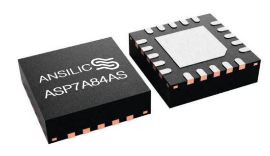
This paper uses the Guoke Anxin ASP7A84AS as a device-level reference to discuss power supply design for low-voltage core rails. The reason for selecting this device is that its datasheet specifications—3A output, 0.8V minimum output, 300mV@3A maximum dropout, QFN20 package, and commercial aerospace-grade irradiation ratings—cover the core parameter dimensions of FPGA core rail power supply. Section 2 decomposes scenario requirements; Section 3 organizes the parameter spectrum and discusses the physical constraints of low-dropout design; Section 4 develops application analysis of input margin, thermal and efficiency, transients and decoupling, sequencing and monitoring, and protection and redundancy; Section 5 discusses synergistic hardening under irradiation conditions; Section 6 presents conclusions. The position of this paper is that the value of a power supply device must be judged through a triple mapping of "load—environment—mission," and discussing power supply specifications divorced from core rail load characteristics has no engineering significance.
(I) Electrical Characteristics of Intelligent Processing Loads
The core power supplies of modern FPGAs and ASICs exhibit three notable characteristics. The first is the coexistence of low voltage and high current: core voltages in advanced processes have dropped to 0.8 V to 1.0 V, while single-device core currents can reach several amperes, and the DC accuracy of the supply rail must be accounted for at the millivolt or even sub-millivolt level. The second is a high current slew rate: logic arrays toggle synchronously on clock edges, load current jumps on nanosecond to microsecond timescales, and the current slew rate can reach several amperes per microsecond; if the target impedance of the power distribution network is too high, transient currents will produce voltage droop across the inductance of the supply path, triggering timing violations or even resets. The third is strong fluctuation in task duty cycle: intelligent inference tasks are bursty, and the payload may remain for long periods in a standby-wakeup-inference-return cycle, with the average and peak load currents differing by an order of magnitude; the power supply device must remain stable over a wide load range and maintain acceptable quiescent current at light load.
Compared with analog loads such as optical focal planes, digital core loads have a different mechanism of sensitivity to power supply noise. Analog loads are concerned with the integral of noise spectral density within the signal bandwidth; digital loads are more concerned with the transient deviation of the supply voltage within the timing window and with power-supply-induced jitter. Periodic ripple on the supply voltage modulates clock path delay, manifesting as clock jitter and reduced setup/hold time margin; broadband noise may couple through the power network into phase-locked loops and high-speed interfaces. Therefore, the evaluation metrics for core rail power supply should focus on "transient deviation, ripple spectrum, and target impedance" rather than low-frequency noise alone.
Projecting scenario requirements onto device parameters yields the following dimensions. The first is voltage and accuracy: the DC accuracy of the core rail is typically required to remain within ±1% to ±2% over the full load range, including initial accuracy, line regulation, load regulation, and temperature drift. The second is dropout and input margin: low-voltage outputs mean that the available voltage difference between the input rail and the output rail is extremely limited, and the device's undervoltage lockout and dropout specifications together determine the minimum input voltage. The third is transient response and decoupling: load steps on the core rail require the output capacitance, equivalent series resistance, and loop bandwidth to be matched, and transient metrics not quantified in the datasheet must be confirmed through measurement. The fourth is thermal and efficiency: in a vacuum environment, heat dissipation is dominated by conduction, and junction temperature is determined jointly by dissipated power, package thermal resistance, and mounting thermal resistance; the efficiency of a linear regulator is approximately the ratio of output voltage to input voltage, and each step increase in the input rail raises dissipation accordingly. The fifth is sequencing and monitoring: the coordination of multi-rail power-up sequencing, soft-start slope, power-good signals, and reset logic determines whether the payload can start reliably; in-orbit observability depends on voltage, current, and temperature telemetry. The sixth is radiation and reliability: total ionizing dose affects parameter drift, single-event latchup and single-event upset affect power supply continuity, and single-event transients may disturb digital logic through the power network. The seventh is size and integration: the core rail power supply should be placed as close as possible to the load to minimize supply path impedance, which imposes dual requirements on package size and thermal dissipation method.
3. Parameter Spectrum and Low-Dropout Constraints of the ASP7A84AS
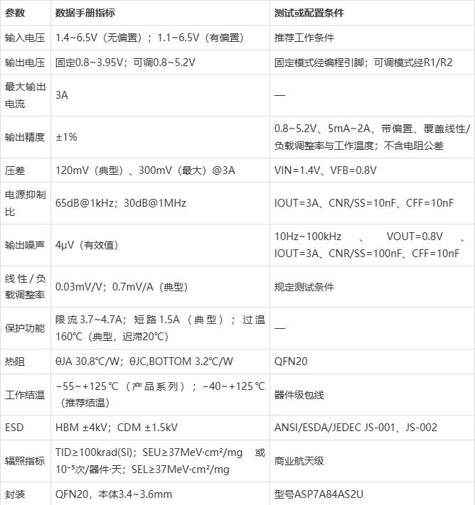
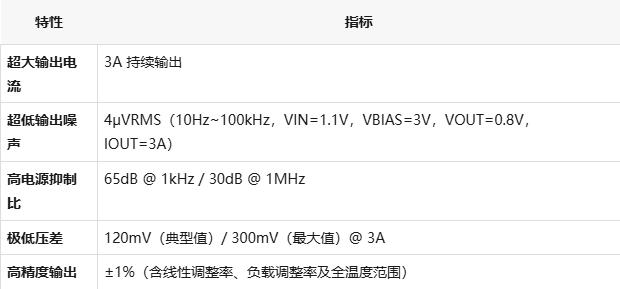
The ASP7A84AS is a 3 A output low-dropout linear regulator with an input voltage range of 1.4 V to 6.5 V without bias and 1.1 V to 6.5 V with bias; the output voltage is fixed at 0.8 V to 3.95 V in the fixed configuration and 0.8 V to 5.2 V in the adjustable configuration; the maximum dropout at 3 A load is 300 mV, with a typical value of 120 mV. The device is packaged in QFN20, the product series is marked with a temperature grade of −55°C to +125°C, the junction temperature range in the recommended operating conditions table is −40°C to +125°C and must be confirmed at the low-temperature end against batch data, and the radiation specifications are TI D ≥ 100 krad(Si), SEU ≥ 37 MeV·cm²/mg or 10⁻⁵ events/device·day, and SEL ≥ 37 MeV·cm²/mg, with the product series model ASP7A84AS2U marked as commercial aerospace grade. For core rail power supply, the following set of constraining parameters is more meaningful: output accuracy of ±1% corresponds to 0.8 V to 5.2 V output, 5 mA to 2 A load, with bias, and covers line and load regulation and operating temperature, excluding external resistor tolerance; the overcurrent protection threshold is 3.7 A to 4.7 A; the short-circuit current is typically 1.5 A; the overtemperature protection threshold is typically 160°C with 20°C hysteresis; the thermal resistance θJA is 30.8°C/W and θJC,BOTTOM is 3.2°C/W; the soft-start time is determined by the NR/SS capacitor, with 10 nF corresponding to approximately 1.28 ms and 100 nF corresponding to approximately 12.8 ms.
Table 1 Key Parameters for Core Rail Power Supply (Based on Datasheet V1.0)
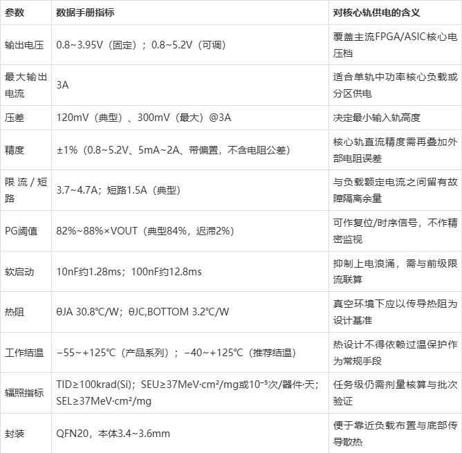
The first constraint on core rail power supply comes from dropout voltage and undervoltage lockout. Taking a 0.8V core rail at 3A full load as an example, the datasheet specifies a maximum dropout voltage of 300mV, meaning the input rail must be at least 1.1V; meanwhile, under biased conditions, the input undervoltage lockout threshold is 1.09V maximum. Combined, a 1.1V input sits exactly at the dual boundary of "dropout just satisfied, UVLO just crossed," and any input droop, ripple, or temperature drift may cause output instability or device shutdown. Therefore, in engineering practice, 1.1V should not be used as the nominal input for the core rail; instead, a 1.2V or higher intermediate rail should be selected, or a 1.1V rail with sufficient dynamic margin provided by the upstream switching power supply should be accepted. The datasheet also specifies: the UVLO threshold is 1.39V maximum without bias, and the bias voltage range is 3V to 6.5V; if the system cannot provide a bias rail, the input rail must be above 1.39V, which significantly alters efficiency and thermal design.
Another implication of low-dropout design is the cost in efficiency. For a linear regulator, the input current is approximately equal to the output current, and efficiency is approximately VOUT/VIN. A 0.8V core rail powered from a 1.2V intermediate rail yields approximately 67% efficiency; from 1.5V, approximately 53%; from 1.8V, approximately 44%. For a 3A load, the dissipated power is 1.2W, 2.1W, and 3.0W respectively (excluding ground pin current). On a benchtop at room temperature, 2W to 3W of dissipation can be handled through copper pours and forced air cooling; in a vacuum environment, the same dissipation must be removed by conduction, and thermal design difficulty rises significantly. The datasheet's θJA=30.8°C/W is based on specific JEDEC board conditions; in vacuum, the convection term disappears, and this value is not directly applicable. Design should start from θJC,BOTTOM=3.2°C/W, superimpose PCB copper spreading thermal resistance, mounting interface thermal resistance, and structural thermal resistance, calculate the total thermal resistance from junction to heat sink surface, and then back-calculate the allowable dissipation based on a 125°C junction temperature limit.
IV. Application Design Analysis for Intelligent Processing Payloads
(I) Input Rail Selection and Thermal–Efficiency Trade-off
Combining thermal boundaries with input margin yields a quantitative method for input rail selection. Let ambient temperature be TA, junction temperature limit be 125°C, total junction-to-ambient thermal resistance be R, and allowable dissipation PD,max=(125°C−TA)/R. Using the datasheet θJA=30.8°C/W for a conservative estimate: when TA=60°C, allowable dissipation is approximately 2.11W; after deducting the contribution of input current and quiescent current, the 1.5V-to-0.8V scheme allows approximately 2.10W for the load, corresponding to 2.1W dissipation at 3A load, already at the critical limit; the 1.8V-to-0.8V scheme corresponds to 3.0W, exceeding by approximately 0.9W, and the output current must be reduced to approximately 2.1A or the input rail lowered. When TA rises to 70°C, allowable dissipation drops to approximately 1.79W, and even the 1.5V-to-0.8V scheme cannot operate at 3A. This set of calculations demonstrates that in core rail power supply, the "3A rating" must be interpreted jointly with "input rail height, ambient temperature, and thermal resistance"; citing the three separately is the most common distortion mode for promotional specifications.
There are three feasible architecture strategies. First, minimize the intermediate rail to the lowest usable value: for example, using a 1.2V intermediate rail to supply a 0.8V core rail yields approximately 67% efficiency, approximately 1.2W dissipation at 3A, and a junction temperature of approximately 97°C at 60°C ambient, leaving approximately 28°C margin. Second, adopt a two-stage structure of "switching power supply coarse regulation + linear post-stage fine regulation": the switching power supply handles most of the voltage drop and maintains high conversion efficiency, while the linear post-stage bears only 0.2V to 0.3V dropout, balancing efficiency and low noise. Third, partition power supply by load: place core logic, transceivers, and interfaces on separate power rails, each supplied by a separate LDO; as per-rail current decreases, thermal design difficulty decreases accordingly, at the cost of increased device count and board area. The three strategies are not mutually exclusive; actual systems often combine them. The selection basis should be the thermal budget and reliability weighting under the mission profile, not a single efficiency figure.
(II) Load Transient and Power Distribution Network Design
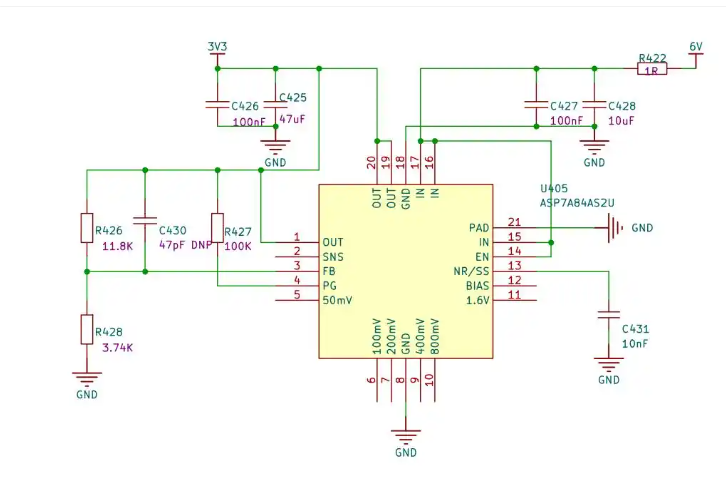
The datasheet provides typical response curves for 0.1 A to 2 A load steps and linear transient curves for 1.4 V to 2.4 V input steps, but does not give numerical transient deviation and recovery time specifications. This information structure dictates the design method: transient performance must be confirmed through measurement or board-level simulation and cannot be directly extrapolated from the datasheet. For the FPGA core rail, it is recommended to establish the power distribution network according to the following steps. First, estimate the target impedance target value based on the load current step amplitude and the allowable voltage deviation (allowable deviation divided by current step). Second, select the output capacitance and equivalent series resistance; the datasheet requires an output capacitance of no less than 22 μF and recommends 47 μF low-ESR X7R ceramic capacitors, and the actual value must be calculated jointly with the target impedance. Third, configure the feedforward capacitor; the datasheet recommends connecting a 10 nF capacitor between FB and OUT to optimize AC performance; increasing the feedforward capacitance can improve transients, but excessive values may affect loop stability and must be confirmed by scanning on the prototype. Fourth, optimize the layout to minimize the loop area among the output capacitor, load input capacitor, and device pins, and keep power traces short and wide to reduce parasitic inductance.
Transient verification conditions should cover the real mission profile: the current step rate, duty cycle, and repetition frequency of inference tasks are usually higher than general test conditions and may be superimposed with other pulsed loads on the satellite (such as payload shutters, cryocoolers, and transmitters). During testing, the load-end voltage, LDO input-end voltage, and current waveforms should be recorded simultaneously to distinguish the portion of transient deviation originating from the LDO loop from the portion originating from collapse of the upstream intermediate rail. If the transient deviation mainly comes from the intermediate rail, the optimization target should be the loop and energy storage of the upstream converter rather than the LDO itself; this is the most common misjudgment in debugging hybrid architectures. For payloads that cannot be repaired in orbit, it is recommended to retain voltage and current telemetry points in the power distribution network and include statistical information on transient events in the telemetry packet to provide data for in-orbit health assessment.
Intelligent processing payloads usually contain multiple power rails such as core, auxiliary, interface, and memory, and the power-up sequence is jointly constrained by the device datasheet and system timing. The EN pin of the ASP7A84AS can be directly controlled by digital logic, with VIH from 1.1 V to 6.5 V and VIL from 0 V to 0.4 V, and interface current within ±0.5 μA; PG is an open-drain output with a typical threshold of 84% and 2% hysteresis, and requires pull-up through a 10 kΩ to 100 kΩ resistor. A typical sequence in engineering practice is: after the intermediate rail is established and confirmed by the upstream PG, enable the core rail and auxiliary rail in sequence; after the core rail PG is valid, release the FPGA reset, and finally enable the interface rail and clock. The selection of the soft-start capacitor must be calculated jointly with the load capacitance and the upstream current-limit value: the datasheet formula is tSTARTUP=1.25×VNR/SS×CNR/SS/INR/SS, where VNR/SS is typically 0.8 V and INR/SS is typically 7.8 μA; 10 nF corresponds to 1.28 ms, 47 nF to approximately 6.0 ms, and 100 nF to approximately 12.8 ms. If the FPGA power-up inrush is large, 47 nF to 100 nF can be selected to spread the inrush current over several milliseconds and avoid triggering current-limit protection in the upstream converter.
Monitoring design should distinguish between "timing signals" and "measurement signals." PG only indicates whether the output voltage has crossed the 84% threshold and has limited amplitude information; it is suitable as a reset-release condition but not for in-orbit health assessment. The latter should be implemented through independent resistor-divider sampling and an analog-to-digital converter, and the sampling points are recommended to cover three locations: the LDO input end, output end, and load end, so as to distinguish input droop from output loop problems. The device has an output active discharge function; after EN is pulled low, the output is discharged through an internal resistor of several hundred ohms, which facilitates rapid power-down and re-power-up. However, the datasheet explicitly warns that when the input voltage is lower than the output voltage, active discharge must not be relied upon to release the charge of a large output capacitor, as reverse current may damage the internal power MOSFET. In dual-rail switching, backup power supply, and ground test scenarios, this constraint must be written into operating procedures.
Thermal design in a vacuum environment should follow the principle of "conduction as the sole path." The exposed pad of the QFN20 package is the primary thermal outlet; the datasheet requires it to be connected directly to the PCB ground plane with copper area maximized, and recommends wide, thick copper for power traces. For the 3A core rail, the following measures are recommended: first, place a via array beneath the pad to conduct heat to inner or backside copper; second, locate the LDO in a thermally stable region of the payload structure to avoid thermal coupling superposition with heat-generating devices such as the FPGA and power converters; third, use thermal interface materials at the mounting interface to compress interfacial thermal resistance; fourth, conduct thermal vacuum tests during the prototype phase to measure junction or case temperature and back-calculate actual thermal resistance, rather than relying on the datasheet θJA. Regarding derating, it is recommended to derate junction temperature, output current, and input voltage per commonly used aerospace derating guidelines, keeping steady-state junction temperature below the recommended upper limit with margin retained; overtemperature protection (typical threshold 160°C, hysteresis 20°C) should serve only as a fault fallback, not as a routine heat dissipation method.
Attention must also be paid to the effect of temperature on accuracy. The datasheet's output accuracy of ±1% covers the operating temperature range, but its test conditions include bias, load from 5mA to 2A, and exclude resistor tolerance; if the core rail uses an adjustable output mode, external resistor tolerance, temperature coefficient, and the FB pin's ±100nA leakage current will add to the total error. Taking 0.8V output as an example, the FB leakage current relative error depends on the divider current: approximately 0.047% at a divider current of 214μA, rising to 0.47% when the divider current drops to 21.4μA. For sub-volt core rails, it is recommended to prioritize a fixed output configuration to confine accuracy attribution to the device itself; when adjustable output is truly needed, low-temperature-coefficient, tight-tolerance resistors should be selected, and the divider network error should be calculated under worst-case conditions.
Failure modes of the core rail can be categorized into four types: overcurrent, short circuit, overtemperature, and single-event-induced. The ASP7A84AS's overcurrent protection limits output current to 3.7A to 4.7A, short-circuit current is typically 1.5A, and overtemperature protection shuts down when junction temperature exceeds 160°C and automatically restarts after cooling by 20°C. These mechanisms cover most electrical faults but cannot cover the following scenarios: prolonged current limiting due to a local short circuit on the load side, output undervoltage due to input rail droop, and short-term output disturbance due to single-event transients. At the systems engineering level, a layered strategy is recommended: the first layer uses current limiting and short-circuit protection to confine fault current to a tolerable range; the second layer uses PG and independent voltage monitoring to trigger load reset, preventing digital logic from misoperating under undervoltage conditions; the third layer adopts dual-rail redundancy or partitioned power for critical processing units, so that a single LDO failure results in degraded operation rather than total payload failure; the fourth layer identifies degradation trends through current telemetry and on-orbit statistical analysis to inform mission planning.
Redundancy design must also account for the costs of mass, volume, and heat dissipation. Dual-rail redundancy means two sets of LDOs and decoupling networks, roughly doubling quiescent power consumption and board area; for micro/nano satellites with tight power budgets, a more realistic approach is "functional partitioning + fault degradation": supplying the core computing domain and interface domain separately, so that if either rail fails, basic telemetry and safe mode are retained pending ground commands. The effectiveness of such strategies depends on the joint design of the power architecture and software strategy, rather than simply increasing the number of devices.
The ASP7A84AS datasheet specifies commercial aerospace-grade radiation metrics of TID ≥100krad(Si), SEU ≥37MeV·cm²/mg or 10⁻⁵ events/device·day, and SEL ≥37MeV·cm²/mg. For intelligent processing payloads, the radiation problem is twofold: on one hand, single-event upsets in the FPGA and memories themselves must be handled by mechanisms such as configuration scrubbing, error-correcting codes, and triple modular redundancy; on the other hand, the power network that provides energy and reference for these mechanisms may also be disturbed by single-event effects. Sensitive nodes of linear regulators include the error amplifier, bandgap reference, and protection logic; single-event transients may manifest as momentary output droop or overshoot, while single-event latch-up may cause a sudden increase in input current. The SEL and SEU thresholds given in the datasheet serve as design and screening criteria, but at the mission level, tests should still be conducted in conjunction with orbital flux, shielding layout, and device lot: for total dose, biased irradiation under a cobalt source or proton source can be performed to examine degradation of output voltage, quiescent current, and regulation; for single events, output waveforms and current can be monitored under heavy-ion or proton beams to distinguish recoverable transients from latch-up states.
System-level hardening is as important as device-level specifications. Recommended measures include: first, configure sufficient decoupling capacitors at the LDO output to provide local charge buffering for single-event transients, preventing disturbances from being directly conducted to the FPGA core; second, power the power monitoring and watchdog logic independently from the monitored power supply to prevent common-cause failures; third, design safe modes in the mission software so that when sustained undervoltage or current anomalies are detected, non-critical payloads are shut down while telemetry and recovery channels are preserved; fourth, adopt a "compute—verify—rollback" process for critical mission phases so that the effects of single-event disturbances can be identified and corrected on the ground or onboard. It should be emphasized that datasheet radiation specifications do not replace batch testing and system verification; the value of commercial aerospace-grade devices lies in front-loading radiation design to the device level, thereby reducing the complexity and cost of system-level hardening—not in eliminating system-level evaluation.
On-orbit intelligent processing pushes the value chain of commercial aerospace from "transmitting data" to "transmitting results," and also pushes the core power supply of FPGAs and ASICs to the forefront of system design. Using the ASP7A84AS as a device-level reference, this paper analyzes three core contradictions in low-voltage core rail power supply: the contradiction between dropout voltage and input margin, the contradiction between efficiency and thermal dissipation, and the contradiction between transient performance and on-orbit verifiability. The device's 3A output, 0.8V minimum output, 300mV@3A maximum dropout, 120mV typical dropout, ±1% accuracy, and commercial aerospace-grade radiation specifications provide a usable design starting point for 0.8V to 1.2V core rails; however, the conditions under which these parameters hold—input rail headroom, ambient temperature, thermal resistance path, external resistor tolerance, and test conditions—must be incorporated item by item into the design documentation. For intelligent processing payloads, the ultimate evaluation criterion for the power architecture is not the parameter levels of a single LDO, but rather "whether, under the mission profile, the core rail voltage always falls within timing margins, whether the junction temperature always falls within the derating range, and whether single-event disturbances can always be identified and recovered by the system." Only by answering these three questions clearly can computing power onboard have a solid energy foundation.
Review of Low-Noise Voltage Regulators for Focal Plane Power Supply Chains in Commercial Optical Remote Sensing Payloads — Using Guoke Anxin ASP7A84AS 3A Low-Dropout Linear Regulator as the Device Reference
LD1085V 3A Low-Dropout Linear Regulator (LDO)
Technical Details of Commercial Aerospace Low-Noise High-Current LDO Chip ASP7A84AS
Lixin Micro ET5C108 Debuts: 3A High-Current LDO Reshapes the Performance Benchmark for Domestic Low-Voltage Regulators
Research on Radiation-Tolerant Power Supply Technology for Precision Instruments in Satellite Navigation and Attitude Control — Power Supply Application Analysis for High-Precision Analog Circuits Based on ASP7A84AS
Research on Low-Noise Power Management Technology for Aerospace Optical Remote Sensing Imaging Systems — Radiation-Tolerant LDO Application Analysis for High-Resolution Imaging Payloads
Guoke Anxin ASL8522S Released: Commercial Aerospace-Grade Precision Operational Amplifier Achieves Key Domestic Breakthrough
Guoke Anxin ASL8522S Released, Filling the Domestic Gap in Commercial Aerospace-Grade Precision Operational Amplifiers
Research on Power Supply Architecture for Digital Processing Units in Commercial Aerospace Communication Payloads — Technical Analysis of High-Precision Low-Dropout Linear Regulators Based on ASP7A84AS
ASP7A84AS — Aerospace-Grade Low-Noise High-PSRR Linear Regulator
Technical Architecture and Multi-Dimensional Performance Characterization of ASP7A84AS Commercial Aerospace-Grade Low-Dropout Linear Regulator
How Low-Noise LDOs Solve Power Supply Challenges in Test & Measurement and Medical Imaging
Guoke Anxin Launches Commercial Aerospace-Grade Low-Cost Radiation-Tolerant LDO Chip ASP7A84AS
Application Analysis of Commercial Aerospace-Grade Radiation-Tolerant MCUs and Power Chips in Silicon Microstrip Detector Systems
Full Development Process of Aerospace-Grade Radiation-Tolerant Power Chips: 10 Core Stages from Design to Market Launch