ZYNQ VDMA Captures OV5640 Video Data and Displays via HDMI
Debugging the OV5640 on ZYNQ and displaying it via HDMI was truly a tale of blood, sweat, and tears!! Am I right!! A tiny camera took me 4 days to debug. Therefore, I'm going to write down this painful experience along with all the lessons and details, as a record of the arduous journey of learning ZYNQ.
When searching Baidu for keywords like ZYNQ VDMA OV5640, most results come from MiLianKe tutorials. I'd like to express special thanks and deep respect to companies and organizations such as MiLianKe, ALINX, Zhengdian Atom, and others, because they provide free tutorials to the many newcomers just entering the ZYNQ world. The blogs from these predecessors also explain clearly the configuration of VDMA, VTC, Video Out, Video In modules and the VDMA registers, so this article will not describe these module configurations in detail. Additionally, many blog posts cover Genlock and Dynamic Genlock explanations; this article only quotes the original text from other tutorials for these two concepts.
These tutorials and methods are essentially paraphrases and summaries of the official UG, PG, and other reference materials.
If you want to build a simple camera capture system using the ZYNQ series, you first need camera example code and documentation. Whether it's STM32 F4 or Cyclone4 FPGA, whether it's ZYNQ example code or the OV5640 Auto Focus Module Application Guide (DVP Interface), such materials are all very important. Because these examples and documents can greatly reduce the work you need to do on initialization.
In addition to the above materials, you also need to understand: the IIC or SCCB communication protocol — ideally you should have experience writing IIC timing yourself (whether you've bit-banged IIC on a 51 microcontroller or simulated IIC on STM32, or better yet on FPGA); the most basic camera timing issues, such as the timing between VSYNC, HREF (shared with HSYNC pin), PCLK, RESET, PWDN, XCLK, and most importantly the data pins; you need to know what RGB888 and RGB565 are, and how RGB565 is converted to RGB888; you need to know the concept of frame buffering and why frame buffers are needed; you need to understand the principle of Dynamic Genlock; and you must know the biggest differences between AXI4-Lite, AXI4-Full (AXI4), and AXI4-Stream (you don't need to understand the specific timing for now).
This article is divided into the following 7 parts to describe this simple experiment:
Using EMIO to emulate SCCB and configure the OV5640.
The basic framework of VDMA and the concepts of frame buffering and Dynamic Genlock.
Completing the initialization of the OV5640 module and VDMA IP in SDK.
Step 1: Using EMIO to emulate SCCB and configure the OV5640.
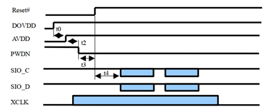
SCCB and IIC transmit single-byte data in exactly the same way, except in the ACK part, there is no need to detect whether the acknowledge signal is high or low (but the clock signal still exists, meaning transmitting one byte requires 9 clock cycles). SCCB does not support multi-byte transfers.
For the OV5640, whose register addresses are two bytes, the SCCB read/write timing is as follows:
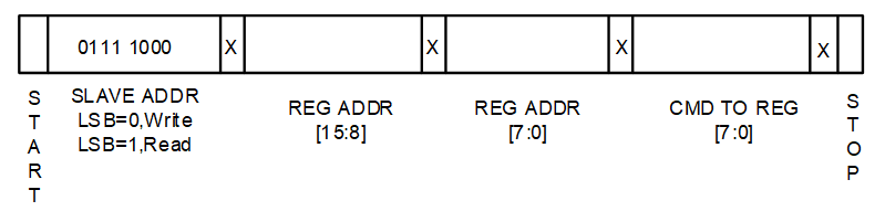

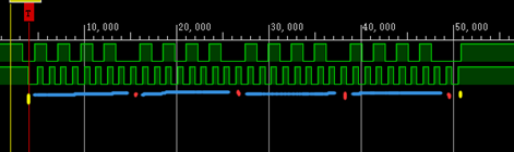
Due to space limitations, I won't post the code here. I believe those who have made it this far won't have much trouble configuring SCCB with EMIO. Of course, you can leave your email in the comments, and I'll send you the entire project when I see it. If you're in a hurry, you can click here to download (and I'll earn some points along the way ^_^). If you want to use ILA to capture the timing of SDA and SCL, it's recommended to add the GPIOs corresponding to these two signals to Debug after Vivado synthesis.
Writing 0xaa to register 0xaa of the device with SlaveAddr 0xaa (ILA capture):
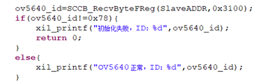
Of course, during initialization, you can also verify whether SCCB is working correctly using the method below. As shown in the figure:
Once SCCB is understood, OV5640 needs to be configured. Configuring the OV5640 essentially comes down to understanding how those 200-plus registers are set. If you have a reference design with suitable resolution and frame rate, that is ideal. You can simply use the registers and configuration parameters provided by the reference design and make minor modifications to the code format. Here I used the ALINX OV5640 pre-configured 1280*720@60Hz reference design. Therefore, the PLL and PCLK sections can be left alone, because configuring the PCLK frequency is quite a troublesome task (there are one or two blog posts on CSDN and Blog Garden that show flowcharts for how to configure PCLK on the OV5640 — in short, it is quite troublesome, so I will not mention it here).
If your camera eventually captures an image but you find the colors are inverted (e.g., blue and red are swapped), you can configure register 0X4300 to select the output color order. In addition, for line timing it is recommended to use HREF (note the difference between HREF and HSYNC).
Step 2: The basic framework of VDMA, and the concepts of frame buffering and Dynamic Genlock
Having discussed VDMA (video direct memory access) at length above, what exactly does the VDMA block diagram look like? Actually, from the English term itself it is not hard to infer — video data interacts directly with memory. Here are the technical terms: VDMA is used to convert AXI Stream-format data streams into Memory Map format, or to convert Memory Map-format data into AXI Stream data streams. In other words, the VDMA core is designed to provide video read/write transfer functionality from the AXI4 domain to the AXI4-Stream domain and vice versa, thereby enabling high-speed data movement between system memory (primarily DDR3) and AXI4-Stream-based target video IP. The block diagram is shown below:
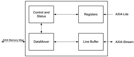
At first glance this system block diagram feels quite frustrating, doesn't it! I clearly remember that various teaching platforms say AXI4-Stream cannot perform memory mapping. Since buffered data needs to be read and written, I accepted that VDMA includes AXI4-Full. Now AXI4-Full has brought along its sibling AXI4-Lite as well. But that is fine — from the diagram, AXI4-Lite is used to configure the VDMA registers, and the data in these registers can control the VDMA's operating mode while also indicating the VDMA's operating status.
AXI4-Lite can program (configure) the IP's registers, thereby enabling software to dynamically configure the VDMA. After programming the registers through the AXI4-Lite interface, the control/status logic block generates the appropriate commands for the Data Mover to initiate write and read commands on the AXI4 master interface. A configurable asynchronous line buffer is used to temporarily hold pixel data before writing it to the AXI4-Memory Map interface or the AXI4-Stream interface.
The VDMA data interface can be divided into two channels: read and write, which operate independently. Through the write channel, users can write AXI-Stream type data streams into system memory (primarily DDR3). In the read channel, the VDMA uses the AXI4 master interface to read data from system memory and outputs it on the AXI4-Stream master interface. As can be seen, the VDMA is essentially a data movement IP that can be regarded as a high-performance DMA with frame buffer functionality specially optimized for video image processing, providing a convenient solution for data entering and leaving system memory. The VDMA core not only has frame buffer functionality but also integrates video-specific features such as Gen-Lock and frame synchronization for fully synchronized frame DMA operations and 2D DMA transfers. In addition to synchronization, frame store numbering and scatter gather or register direct mode operations can be used for central processor control. In this design, the VDMA scatter gather function is not used because the system can be fully implemented using the simpler register direct mode of the VDMA, thereby avoiding the area cost associated with implementing the scatter gather function. Scatter gather should only be enabled when the system requires relatively complex software control of the VDMA. (Quoted from ALIENTEK tutorial)
2. Frame Buffer (original text from ALIENTEK tutorial)
First, let us look at what a frame buffer is. Frame Buffer memory, abbreviated as frame buffer and often also called video memory, is a storage area that provides data buffering for display devices (such as HDMI monitors, RGB LCD screens, etc.). Generally, the transmission rates of the image input source and image display do not match (e.g., the image input source transmission speed is faster or the image display side transmission speed is faster). At this time, a storage area is needed to buffer the input data so that the display device can read the data, and also to facilitate subsequent image processing of the video data. Each storage unit of the frame buffer corresponds to one pixel on the screen, and the entire frame buffer corresponds to one frame of image.
In practical applications, external DDR3 memory is generally chosen as the frame buffer rather than on-chip BRAM, because the on-chip BRAM storage capacity of ZYNQ is very small. As we know, the BRAM storage capacity of ZYNQ7010 is 2.1 Mbit, and the storage capacity of ZYNQ7020 is 4.9 Mbit. Assuming the resolution of an RGB LCD screen is 800*480, the storage capacity required to store one frame of image is (e.g., RGB888 data format = 24 bits): 800*480*24 = 9,216,000 bit ≈ 8.79 Mbit. The entire BRAM storage capacity is insufficient to store a single frame of image, let alone situations where more frame buffers are sometimes needed. Therefore, external DDR3 memory is used as the frame buffer.
For using frame buffer memory to buffer image data, either single-frame buffering or multi-frame buffering schemes can be adopted. Single-frame buffering means that both the image input and the image display are realized by reading and writing the same storage area. Although this can also realize the function of the display device displaying images, it brings about a problem: the single frame of image read out is the result of two or more frames of input image data superimposed together, which may cause the image displayed on the display device to appear torn. The read/write diagram of the single-frame buffering scheme is shown in the figure below:
In view of the disadvantage of image tearing in single-frame reading as shown in the above figure, using double (multiple) buffering can avoid this situation. In most cases, using 3 display buffers is the best choice. The double buffering mode is shown in the figure below:
Concept of Dynamic Genlock:
In many video applications, the data rates of the image input end and output end do not match, and frame buffers are usually used to avoid potential errors caused by rate mismatch. To solve the image superposition problem caused by a single frame buffer area, multiple frame buffer areas are allocated to store data. When the image input end is writing to one of the frame buffers, the output end reads from the other frame buffers. So what is Genlock? The meaning of this term is synchronous lock.
This so-called genlock is actually used in VDMA; the so-called synchronization means that the displayed image only follows the data captured by the camera (with only a one-frame difference, which can be regarded as synchronization in the real world; do not compare this with synchronization such as reset). Our predecessors were truly remarkable and invented many synchronization methods. Xilinx's VDMA has 4 synchronization modes:
① Genlock Master: When the write channel (S2MM) or read channel (MM2S) is configured as Genlock Master, that channel will not skip or repeat any frame buffer region and reads data in frame buffer order. A channel configured as Genlock Slave should closely follow changes in the Genlock Master channel, but with a certain delay, the size of which is configured in the register (*frmdly_stride[28:24]).
② Genlock Slave: When the write channel (S2MM) or read channel (MM2S) is configured as Genlock Slave, that channel attempts to synchronize with the Genlock Master channel by skipping or repeating some buffer regions.
Illustration: The figure below shows the configuration in Genlock mode, where S2MM is Master and MM2S is Slave, and the Slave closely follows the memory (red and purple) that the Master has finished operating on. In order to closely follow the Master, the Slave may skip frames. As shown at the boundary between red and purple for the Slave in the figure, a jump from 0 to 2 occurs, and buffer 1 is not read; in addition to this phenomenon, at the blue marked location there is also a phenomenon in which the Master and Slave operate on the same buffer together.
(Personal speculation: who should be configured as master and who as slave depends on whether writing is faster or reading is faster. Think about it.)
③ Dynamic Genlock Master: When the write channel (S2MM) or read channel (MM2S) is configured as Dynamic Genlock Master, that channel skips the frame buffer currently being operated on by the Dynamic Genlock Slave channel, accomplishing this by skipping or repeating some frame buffer regions. Here, allocating three frame buffers is taken as an example. When the channel configured as Dynamic Genlock Master accesses frame buffers and does not detect the frame buffer being accessed by the Slave channel, it accesses frame buffers cyclically in the order 0 1 2 0 1 2; however, if it detects the frame buffer region being accessed by the Slave, it skips that region and starts accessing the next frame buffer. Therefore, if the Slave channel accesses frame buffer 1 for a long time, the Master will cyclically access frame buffers 2 and 3.
④ Dynamic Genlock Slave: When the write channel (S2MM) or read channel (MM2S) is configured as Dynamic Genlock Slave, that channel operates on the frame that the Dynamic Genlock Master channel operated on in the previous cycle.
Illustration: Red and purple indicate following the buffer from the previous step. However, when the Slave is operating on a buffer region, the Master cannot take what others love and can only skip this buffer and look for the next buffer. This avoids the situation in Genlock mode where the Master and Slave fall in love with the same buffer at the same time. Although frame skipping also occurs, the advantage compared with Genlock mode is obvious. In addition, for real-time displayed video, the Master and Slave operating on the same segment of memory at the same time is itself the fundamental reason for introducing frame buffers. Therefore, in video processing, we need to adopt Dynamic Genlock mode.
The above is the concept of genlock in VDMA. S2MM (my understanding is that whoever writes the data stream into the memory map, therefore it is write-in). MM2S (my understanding is reading from the memory map onto the data stream bus, therefore it is read-out). Memory map, stream.
If you want to use Zynq to drive the OV5640 and transmit the video to a display via HDMI, you might think a simple DVP (OV5640) to RGB (HDMI INPUT) to HDMI OUTPUT conversion would suffice. Honestly, are you trying to skip the AXI4 protocol? If that's really what you think, you're being a bit too naive. Because the clocks of the OV5640 and HDMI are not synchronized—if the clock difference is small, even if display works, it won't show issues in a short time. In addition, the camera does not have the clkx5 clock (clk_x5 for HDMI), so you get the idea—you can't simply do a direct conversion. The actual framework is as follows.
Here we reference the overall framework diagram from the ALIENTEK tutorial (the screenshot is a bit blurry). In this framework diagram, the light yellow parts are the IPs we need to use. How these IPs are designed is something we as beginners don't need to dig into—we just need to know how to use them.
From the diagram, it's easy to see that we need to use 7 main IPs (the configuration of these modules is not covered here; many blogs already mention the configuration of these IPs, see other blogs):
OV5640 image capture IP, which is responsible for converting the data captured by the camera into the AXI4-Stream protocol.
Video in to AXI4-Stream IP—as the name suggests, it is responsible for feeding the captured data into the VDMA.
VDMA IP is the core IP of this design. It can store the video data stream into DDR3, and it can also read the video data from DDR3 and turn it into a video stream. (The core module between frame buffer reads and writes.)
AXI4-Stream to Video out IP—as is easy to see, under the control of the VTC (Video Timing Controller), it can output the video stream to external devices.
VTC controls the output timing of video out.
The dynamic clock is responsible for providing the video core clock signal for the VTC and HDMI.
DVI transmission interface. HDMI is backward compatible with DVI, so the DVI IP is used here, but the actual board interface is HDMI.
Step 4: How the IPs are interconnected.
At first glance, how do you connect so many wires? Actually, there is an inherent pattern.
dynamic clock: the output pixel clock and serial clock connect to DVI, and Locked connects to the reset terminal of RGB2DVI. This ensures that RGB2DVI is not reset while the clock is stable. At the same time, this pixel clock also connects to the video output clock (vid_io_out_clk) of the video out module and the video core clock clk of the VTC (PG016 describes clk as: video core clock).
Connect the HP clock to the AXI-MM2S-ACLK and AXIS-MM2S-ACLK of the VDMA. FCLK0 connecting to AXI_GP0_ACLK goes without saying. The vtg_ce of Video out (PG044 describes vtg_ce as: VTC clock enable. used to halt the timing generator for synchronization purposes) should be connected to the gen_clken of the VTC (the author couldn't find the error on this wire and wasted a lot of time). Personal guess: this way, video out can be ensured to enter the working state in advance and wait for the arrival of video data.
Vtiming_out corresponds to vtiming_in; vid_io_out corresponds to the RGB of rgb2dvi; M_AXIS_MM2S corresponds to the video_in of video out.
The GP clock is low-speed, with a frequency of 50 MHz, so it provides the clock for the configuration interfaces (AXI4-Lite) of each module. The HP interface is high-speed, with a frequency of 100 MHz, and it is the transmission clock for the video data stream. Therefore, connect the clocks of all Lite interfaces to 50 MHz, and connect all data stream interfaces to 100 MHz. Also note that the resets of the Lite interfaces should all be connected to the output reset signal of the 50 MHz module. The resets of the Stream interfaces should all be connected to the output reset signal of the 100 MHz module.
The video input clock of Video in should be connected to the output clock of the OV5640 capture module.
Even if you accidentally connect several clock signals incorrectly or are confused about individual signal types, serious warnings and errors will appear during validation. At this point, you can make corrections based on the prompted information.
Note that the reset signal must not be omitted. Finally, enable automatic connection and verify whether there are serious warnings or errors.
The ACLK of GP and the ACLK of HP are not kept at the same frequency here, meaning Lite and Stream do not use the same clock. Attached is the system diagram with signals connected (zoom in on the PDF in the download link attachment for a clearer view).
Constrain the pins in the normal way. However, one point needs attention: because pclk is an input clock signal, an error will occur when generating the bitstream. Therefore, Vivado needs to know during bitstream generation that this port is a clock signal, so the following needs to be added to the constraint file:
set_property CLOCK_DEDICATED_ROUTE FALSE [get_nets cam_pclk_IBUF]
This way the bitstream can be generated smoothly. If you do not add it, that is also fine; when generating the bitstream, you can modify the error according to the prompt using the method above.
Step 6: Complete the initialization of the camera and VDMA in SDK.
Using the ALIENTEK example and the ALINX board. Of course, you can also configure the registers as in the tutorial provided by MiLianKe (due to space limitations, only the main program is given).
#include"xil_types.h"
#include"xil_cache.h"
#include"xpa ram ete rs .h"
#include"xaxivdma.h"
#include"xaxivdma_i.h"
#include"display_ctrl_hdmi/display_ctrl.h"
#include"vdma_a pi /vdma_api.h"
#include"emio_sccb_cfg/emio_sccb_cfg.h"
#include"ov5640_sccb.h"
#defineDYNCLK_BASEADDR XPAR_AXI_DYNCLK_0_BASEADDR // Dynamic clock base address
#defineVDMA_ID XPAR_AXIVDMA_0_DEVICE_ID // VDMA device ID
#defineDISP_VTC_ID XPAR_VTC_0_DEVICE_ID // VTC device ID
// Starting address of the frame buffer
unsigned int const frame_buffer_addr = (XPAR_PS7_DDR_0_S_AXI_BASEADDR
DisplayCtrl dispCtrl;
VideoMode vd_mode;
vd_mode=VMODE_1280x720;