Xilinx FPGA Input Delay Primitives: IDELAYE2 and IDELAYE3 Explained
In high-speed interface design, timing closure is often the biggest "nightmare" engineers face. When data rates exceed 800Mbps, even minor PCB trace differences can cause system failure. This article provides an in-depth analysis of the underlying principles of Xilinx 7 Series (IDELAYE2) and UltraScale Series (IDELAYE3), helping you thoroughly overcome input delay calibration challenges.

I. Core Fundamentals: Why Do We Need IDELAY?
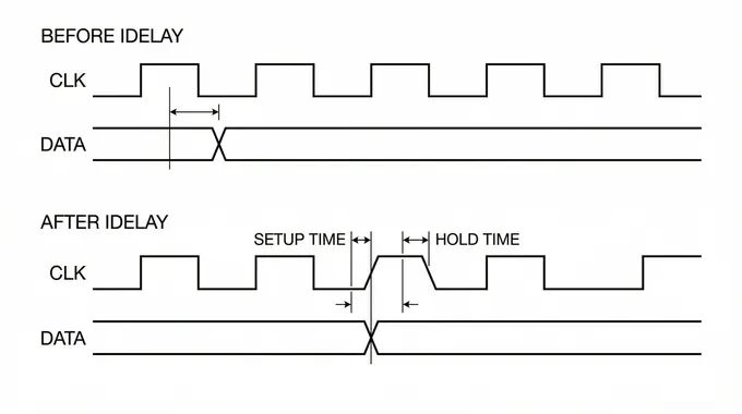
In high-speed systems, signals propagate across the PCB at approximately 6 inches/ns. This means a 100mil trace mismatch equates to roughly 16ps of timing skew. In DDR3-1600, a single data window is only 625ps. If PCB routing cannot achieve absolute length matching, the data eye diagram will close.
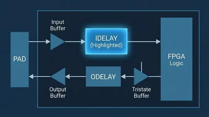
The role of IDELAY is to sit between the FPGA IO Pad and internal logic, precisely controlling the delay line to "fine-tune" the arrival time of input signals at the sub-nanosecond level. Keep these three golden rules in mind during design:
Physical location lock: IDELAY resides inside the IOB, adjacent to the physical pin. Once the signal enters internal routing, it can no longer be used.
Companion relationship: In applications such as DDR, it must be cascaded with ISERDES.
Heart dependency: It must be supplied with a high-precision reference clock by IDELAYCTRL; otherwise, delay accuracy cannot be guaranteed.
II. IDELAYE2 Detailed Explanation (7 Series FPGAs)
For Artix-7, Kintex-7, and Virtex-7, IDELAYE2 is the workhorse. It uses a "Tap" structure with 32 taps total, each tap averaging approximately 78ps delay (affected by the reference clock), with a total delay range of 0 to 2.5ns.
The delay value is fixed at Bitstream generation time and cannot be changed after power-up.
Most commonly used. Dynamically adjusted at runtime via CE/INC ports, used for DDR read balancing.
Allows direct loading of a 5-bit value into the delay line.
Standard dynamically adjustable mode (VARIABLE) instantiation code:
.CINVCTRL_SEL ("FALSE"),
.DELAY_SRC ("IDATAIN"), // Key: signal source comes from IOB pin
.HIGH_PERFORMANCE_MODE ("TRUE"), // Enable high-performance mode to reduce jitter
.IDELAY_TYPE ("VARIABLE"), // Dynamically adjustable mode
.IDELAY_VALUE (0),
.REFCLK_FREQUENCY (200.0), // Reference clock must match IDELAYCTRL
.SIGNAL_PATTERN ("DATA")
.CNTVALUEOUT (cntvalueout), // Outputs current delay value (debugging lifesaver)
.DATAOUT (dataout), // Output to ISERDES
.C (clk),
.CE (ce), // 1=enable adjustment
.IDATAIN (datain), // Input from physical Pad
.INC (inc), // 1=increase delay, 0=decrease
.LD (1'b0),
.REGRST (rst)
III. IDELAYE3 Detailed Explanation (UltraScale/UltraScale+ Series)
In the UltraScale architecture, E3 brings a qualitative leap:
Precision revolution: Native precision improved to 4~10ps, supporting DDR4-2400+.
Native Time Mode: Supports DELAY_FORMAT = "TIME", allowing direct setting of 500ps without manual tap calculation.
VT Auto Calibration (EN_VTC): The FPGA automatically compensates for voltage and temperature drift in the background, ensuring absolute delay stability.
UltraScale IDELAYE3 instantiation code:
.DELAY_FORMAT ("TIME"), // [Highlight] Unit directly in ps
.DELAY_TYPE ("VARIABLE"),
.DELAY_VALUE (100), // Initial delay 100ps
.REFCLK_FREQUENCY (300.0), // Recommended reference clock 300MHz
.UPDATE_MODE ("ASYNC")
.CNTVALUEOUT (cntvalueout),
.DATAOUT (dataout),
.CE (ce),
.CLK (clk),
.DATAIN (datain),
.EN_VTC (en_vtc), // [Core] Enable auto compensation
.INC (inc),
.RST (rst) // Note: E3 uses RST, E2 uses REGRST
4. Comprehensive Comparison: IDELAYE2 vs IDELAYE3
IDELAYE3 (UltraScale)
Case 1: DDR3 Interface Physical Layer (IDELAYE2 + ISERDES)
The core logic is "blind calibration." The FPGA scans through 0~31 Taps via a state machine to find the most stable data point. Note that due to PCB trace differences, each data bit (DQ) must have its own independently instantiated IDELAY.
for(i = 0; i < 8; i = i + 1) begin : gen_delay
.IDELAY_TYPE ("VARIABLE"),
// ... (other parameters) ...
.IDATAIN (dq_in[i]), // Independent input for each bit
.DATAOUT (dq_delayed[i]),
.INC (delay_inc),
.CE (delay_ce),
ISERDESE2 #( .DATA_RATE("DDR"), .DATA_WIDTH(8) ) iserdes_dq (
.D (dq_delayed[i]), // Receive delay-calibrated data
endgenerate Case 2: MIPI D-PHY Interface (IDELAYE3)
Leverage E3's high precision and VAR_LOAD mode for fast alignment.
.DELAY_FORMAT ("TIME"),
.DELAY_TYPE ("VAR_LOAD"), // Allows direct value loading
.DELAY_VALUE (50), // Initial 50ps compensation for PCB skew
.REFCLK_FREQUENCY (300.0),
) idelay_mipi (
.DATAOUT (data_delayed),
.EN_VTC (1'b1), // Keep high to let FPGA automatically resist temperature drift
.LOAD (load_delay),
.CNTVALUEIN (optimal_delay_val) // Directly load algorithm value
1. IDELAYCTRL is mandatory! All IDELAYs within an I/O Bank share the IDELAYCTRL corresponding to that Bank. After system power-up, IDELAYCTRL must be reset first, and then wait for its RDY signal to go high.
2. Clock driving must be clean: The reference clock for IDELAY must never use a regular logic clock; it must use a stable clock generated by BUFG/BUFIO.
3. Multi-channel independence: Do not attempt to use a single IDELAY to control a bus. An 8-bit data bus must instantiate 8 IDELAYs.
Summary: The IDELAY primitive is the FPGA's "ticket" to the high-speed world. The 7 Series (E2) is robust and classic, suitable for DDR3; UltraScale (E3) introduces picosecond-level Time mode and automatic temperature compensation, making it the ideal choice for DDR4 and MIPI.