Six 150-Megapixel Cameras Working Simultaneously: How Does FPGA Handle Nearly 2GB/s Data Torrent?
In high-end industrial equipment, the FPGA challenge is sometimes not about implementing highly complex algorithms, but about how to keep large volumes of data flowing continuously and reliably.
The Leica CityMapper-2, developed by Leica Geosystems, is a typical example. This airborne urban 3D mapping system carries six 150MP cameras and a LiDAR with a 2MHz pulse rate, completing an image acquisition cycle every 0.9 seconds, with the entire system's data transfer rate approaching 2GB/s.
Such a massive data stream must be received through high-speed interfaces, preprocessed, buffered in storage, and ultimately transmitted to the host via PCIe. The greater challenge is that the host runs Windows 10, which is not a real-time operating system. Ensuring precise synchronization of multiple cameras while guaranteeing no frame loss during data transfer places high demands on the hardware architecture and data communication capabilities of the entire system.
To address this, Leica did not choose to design a complex FPGA hardware platform from scratch. Instead, it adopted the Mercury+ XU8 System-on-Module (SoM) from Enclustra, along with Enclustra's FPGA Manager PCIe IP communication solution.
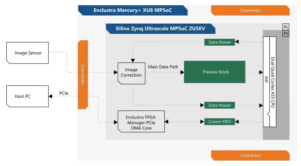
Leica CityMapper MFC150 system architecture diagram
The combination of these two technologies is compelling: the SoM provides an integrated and validated FPGA hardware platform, resolving low-level hardware development issues; the FPGA Manager PCIe IP establishes data communication between the FPGA and the host, addressing high-speed data transfer and hardware-software co-design challenges.
For Leica, this was not merely purchasing an FPGA module, but obtaining a complete solution spanning from hardware platform to high-speed communication. It also demonstrates that as FPGA application complexity continues to increase, the combination of standardized modules, mature IP, and supporting software is becoming an effective path for shortening the development cycle of complex electronic systems.
A nearly 2GB/s data stream tests the coordination capabilities of the entire system
Let us first look at the application scenario of the Leica CityMapper-2.
This is a system designed specifically for airborne urban 3D mapping, collecting urban data through multi-view cameras and LiDAR mounted on an aircraft, ultimately generating high-precision 3D maps and urban digital twin models. Its core imaging system, the Leica MFC150, is equipped with six 150MP cameras, including two nadir-facing RGB/NIR cameras and four RGB oblique cameras, plus an integrated 2MHz pulse rate LiDAR. All camera modules are mounted in a pod weighing 58kg.
The first challenge is multi-camera synchronization. All six cameras must expose at exactly the same moment to ensure temporal consistency across images from different viewpoints. For airborne mapping equipment, even slight deviations in exposure timing can affect subsequent image registration and 3D reconstruction.
The second challenge is high-speed data acquisition and transfer. The data generated by six 150-megapixel cameras must be preprocessed and buffered before being continuously transmitted to the host, with an average data rate approaching 2GB/s.
This places multiple demands on the FPGA system: Can the high-speed image interfaces receive data reliably? How should multiple data streams be organized and scheduled? Can external memory provide sufficient buffering capacity? Can the PCIe link continuously sustain the front-end data stream?
These issues cannot be solved simply by adding more FPGA logic resources.
From an engineering perspective, the entire system needs to establish a reliable data path among the sensors, FPGA, memory, and host. A bottleneck at any stage can affect the overall operating efficiency of the equipment.
Leica determined early in the project that only an FPGA-based approach could meet the system's requirements for high bandwidth, low latency, and high integration. But another decision was equally important: not to design an FPGA board from scratch, but to adopt a proven FPGA SoM.
This set the direction for subsequent system development.
Mercury+ XU8 SoM: integrating a complex FPGA hardware platform
Why did Leica choose not to design its own FPGA board?
For experienced FPGA engineers, there is still considerable work involved before an FPGA chip truly becomes a functioning hardware system. Beyond the chip itself, power supplies, clocks, DDR memory, high-speed interfaces, and various peripheral circuits must be designed. When PCIe, USB 3.0, and high-speed storage interfaces are involved, PCB signal integrity, power integrity, thermal management, and board-level verification must also be considered. This work requires not only a professional hardware R&D team but also repeated prototyping, debugging, and design iterations.
For a professional equipment manufacturer like Leica, R&D resources should clearly be invested more in core business areas such as optical systems, mechatronics, multi-sensor synchronization, and surveying algorithms, rather than repeatedly dedicating substantial effort to underlying FPGA boards. Therefore, Leica chose the Mercury+ XU8 System-on-Module from Enclustra.
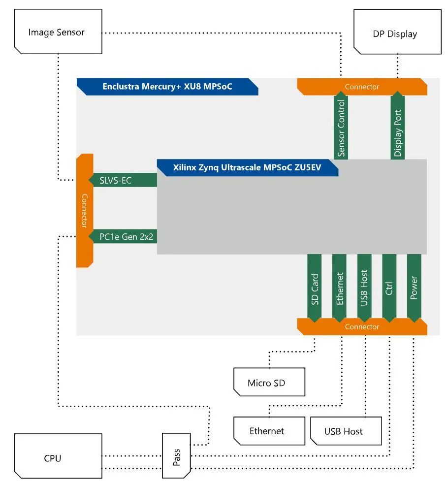
CityMapper functional block diagram based on the Enclustra Mercury+ XU8 System-on-Module
This module is based on the AMD Zynq UltraScale+ MPSoC family and integrates programmable logic, an ARM processing system, and peripheral hardware resources into a standardized module. Its main configuration includes high-speed DDR4 ECC SDRAM, eMMC Flash, Quad SPI Flash, dual Gigabit Ethernet PHYs, and dual USB 3.0 interfaces, forming a complete embedded processing platform.
It is worth noting here that a SoM is distinctly different from simply purchasing an FPGA chip.
After purchasing a chip, customers still need to complete peripheral circuit design, memory interface design, power management, and PCB layout and routing. With a SoM, customers can directly carry out application development on an already integrated hardware platform. This is equivalent to delegating a portion of the complex underlying hardware engineering to a professional module vendor.
In the CityMapper-2 project, the Mercury+ XU8 handles tasks such as multi-channel image data reception, preprocessing, caching, and communication with the host. The ARM processing system on the module is responsible for configuring various functional modules, controlling them via the AXI bus, communicating with the host controller, and managing image acquisition parameters and task workflows.
This division of labor between PS (Processing System) and PL (Programmable Logic) is also an important characteristic of the Zynq MPSoC architecture. The PS handles system control, configuration, and management, while the PL leverages the FPGA's parallel processing capability to complete data processing tasks with high real-time and throughput requirements. For multi-sensor, high-speed data acquisition systems, this heterogeneous architecture can balance control flexibility and hardware processing efficiency.
Of course, the value of a SoM is not limited to hardware integration. Enclustra also provides a Linux Board Support Package (BSP), detailed technical documentation, and reference designs to help customers reduce the workload of platform porting and system debugging. This means Leica does not need to start from the most basic hardware and software adaptation work but can carry out product development on a relatively mature platform.
FPGA Manager PCIe IP: Enabling High-Speed Communication Between FPGA and Host
If the Mercury+ XU8 solves the FPGA hardware platform problem, then the Enclustra FPGA Manager PCIe IP solves another key problem: how to enable efficient communication between the FPGA and the host.
This is especially important in CityMapper-2.
After all, the data acquired by the six front-end cameras ultimately needs to enter a host running Windows 10 and be written to four SSD solid-state drives. Even if the FPGA can complete image reception and preprocessing, without a stable and efficient host communication solution, the entire system still cannot operate smoothly.
Under traditional development approaches, engineers need to handle the FPGA-side PCIe interface logic, host-side drivers, data transfer control, and communication protocols between software and hardware themselves. For high-speed data acquisition equipment, this work is not simple.
The FPGA Manager PCIe IP provided by Enclustra encapsulates this underlying communication work.
This solution consists of two parts: the FPGA-side IP Core and the host-side software library (DLL). Through a unified API interface, user applications can communicate with the FPGA using simple read and write commands, without having to deal with the complex details of the underlying protocol.
Meanwhile, the solution supports two data access modes: Streaming Access, suitable for continuous data stream transmission; and Memory-Mapped Access, which facilitates host access to the memory space and registers mapped inside the FPGA.
For CityMapper-2, what truly plays a key role is the DMA data transfer mechanism within it.
In this architecture, images captured by six cameras enter the FPGA through the SLVS-EC high-speed interface, undergo preprocessing such as image correction, and are temporarily stored in external SDRAM.
Subsequently, the host starts the DMA engine in the FPGA Manager PCIe IP, and data is transferred directly to host memory via PCIe, without requiring the host CPU to participate in data movement transaction by transaction.
If the CPU were involved in every data copy and transfer, a data stream of nearly 2GB/s could easily impose an additional burden on the host. Especially in a non-real-time operating system environment like Windows, the CPU also needs to handle OS scheduling, application execution, and other system tasks.
DMA, on the other hand, delegates the main data movement work to dedicated hardware, reducing CPU involvement and lowering system load.
It should be noted that DMA does not mean the CPU completely exits the data processing process. The host is still responsible for transfer initialization, task management, and status monitoring, but the high-throughput data movement is stripped from the CPU's daily burden.
This is actually a very typical hardware-software co-design approach: tasks with high bandwidth and timing requirements are assigned to the FPGA and dedicated hardware, while control and management tasks are left to the ARM processing system and host software.
In addition, the Mercury+ XU8 integrates an image preview function. During flight, operators can check image quality via an external display to confirm whether data acquisition is functioning properly.
From sensor reception, FPGA preprocessing, and SDRAM buffering to DMA and PCIe transmission, the entire data link forms a relatively complete system architecture.
This is also the core value of the FPGA Manager PCIe IP in this project: it is not just a PCIe interface IP, but through the FPGA-side IP core and host-side software library, it provides customers with a complete host-to-FPGA communication mechanism.
SoM+PCIe IP: From Providing Hardware Modules to Providing Complete Solutions
Looking at the Mercury+ XU8 and FPGA Manager PCIe IP together, one can understand the true value of Enclustra in this project.
The two address problems at different levels, yet are closely related. The SoM solves the hardware platform integration problem, so customers do not have to design complex FPGA boards from scratch; the FPGA Manager PCIe IP solves the host communication problem, so customers do not have to redevelop an entire underlying PCIe communication mechanism and accompanying software.
One provides the hardware foundation, the other provides communication capability. For Leica, this combination means the R&D team can focus more energy on its core business, rather than repeatedly investing in underlying hardware design and interface development.
In fact, this model has very practical appeal for professional industrial equipment manufacturers. Many high-end industrial equipment, test and measurement instruments, and machine vision systems have similar development needs: they need to process high-speed sensor data, require FPGAs to provide deterministic real-time processing capability, and also need high-speed communication with a PC or embedded host.
However, these customers may not want to design FPGA boards from scratch themselves, nor may they be willing to invest substantial resources in developing general-purpose communication IP and drivers. If a supplier can provide both a proven SoM hardware platform and accompanying communication IP, it can help customers save considerable repetitive work.
The Enclustra solution has another noteworthy feature: FPGA Manager is not limited to Enclustra's own modules and can also be applied to customer-designed FPGA systems. This means customers can either choose the integrated SoM + IP solution or introduce its communication IP into their existing hardware platforms. This openness helps expand the application scope of the solution.
From a project economics perspective, Leica also gained tangible benefits. By using standard modules, the development team avoided the need to build numerous prototype boards, repeatedly revise designs, and write complete low-level technical documentation, while also reducing the risk of board-level design errors. What surprised the Leica team even more was that the price of Enclustra standard modules for small-volume requirements was almost close to the cost of purchasing FPGA chips alone. Behind this is the production scale of standardized modules and the supplier's long-accumulated manufacturing and optimization experience.
Daniel Wintsch, head of Leica's electronics development team, stated that Enclustra provided a proven plug-and-play solution that relieved pressure on the development team and allowed them to focus on their own core technologies. This is also an important reason why Enclustra became a long-term supplier to Leica.
For complex industrial equipment, R&D costs are never just the procurement costs of chips and components. Engineering investment, development cycles, repeated debugging, verification risks, and subsequent maintenance are also important components of project costs.
From this perspective, the combination of SoM and PCIe IP brings not only development convenience but also improvements in overall project development efficiency and risk control capability.
FPGA industry competition is shifting from chips to system-level delivery
The Leica CityMapper-2 case has another aspect that deserves more attention from the domestic FPGA industry.
In the past, when discussing FPGA competition, the industry tended to focus on chip metrics such as logic cell scale, DSP count, on-chip memory, SerDes speed, and power consumption.
These are certainly important. But for customers who truly need to deploy FPGAs in products, chip performance is only the starting point. Even if an FPGA chip has sufficient logic resources, without mature interface IP, memory controllers, drivers, and development tools, customers still need to invest substantial engineering resources to complete product development.
Conversely, an FPGA platform with appropriate performance, mature hardware integration, and complete supporting IP may be more readily adopted by customers. Especially in the high-end industrial equipment and professional instrumentation markets, what customers truly need is often not an isolated chip but a solution that can operate stably, integrate conveniently, and be maintained over the long term.
This is why the Enclustra case deserves attention. Through the combination of the Mercury+ XU8 SoM and FPGA Manager PCIe IP, it integrates two key elements—the hardware platform and host communication—lowering the barrier for customers developing complex FPGA systems.
For domestic FPGA vendors, this also offers a direction worth considering.
For domestic FPGAs to enter higher-end industrial, measurement, communications, and data center markets, in addition to continuing to improve chip performance, they need to build more complete capabilities in modular products, interface IP, reference designs, driver software, and technical support. In particular, as customers begin to shift from purchasing individual chips to evaluating system solutions, whether a supplier can provide proven hardware-software combinations may directly affect product adoption efficiency.
Of course, not all applications require standard SoMs. For products with large-scale mass production, extreme cost sensitivity, or special hardware architecture requirements, custom design still has its value. But for professional equipment with tight development schedules, high system complexity, and relatively limited volumes, the combination of mature modules and supporting IP is undoubtedly a path worth considering.
Returning to the Leica CityMapper-2, six 150-megapixel cameras and a data stream of nearly 2GB/s are only the most直观 aspect of this case. What truly deserves attention is how Enclustra, through the SoM hardware platform and FPGA Manager PCIe IP communication solution, integrates complex FPGA hardware integration and high-speed host communication into a complete engineering solution.
The value of FPGAs should not stop at providing programmable logic resources. For industrial customers, the ability to bring FPGAs into final products faster, more reliably, and with lower risk is a more meaningful competitive advantage.
Technical Analysis of 1 GB / 2GB 240-Pin DDR3 SDRAM UDIMM Modules
Technical Analysis of 2GB, 4 GB 240-Pin DDR2 SDRAM FBDIMM
Design Analysis of 1 GB, 2GB 184-Pin DDR SDRAM RDIMM Memory Modules
Technical Analysis of 1 GB / 2GB 184-PIN DDR RDIMM Memory Modules
Technical Analysis of 2GB /4 GB 240-Pin DDR2 SDRAM RDIMM
In-Depth Analysis of 1 GB / 2GB 200-Pin DDR2 SDRAM SODIMM
2GB /4 GB 240-Pin DDR3 SDRAM UDIMM: A Comprehensive Analysis of Design and Application
Detailed Hardware Design of 2GB /4 GB 240-Pin DDR3 UDIMM
Technical Dissection of 2GB /4 GB 240-Pin DDR3 SDRAM UDIMM
In-Depth Analysis of 1 GB / 2GB /4 GB 240-Pin DDR2 SDRAM RDIMM
Technical Analysis of 1 GB / 2GB 240-Pin DDR2 SDRAM FBDIMM
Technical Analysis of 2GB /4 GB 200-Pin DDR2 SDRAM SODIMM Modules