Modulated Signal Demodulation Design Based on ALINX ZYNQ7010 Core Board
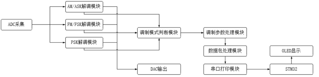
This design is based on the ALINX ZYNQ7010 core board, DAC 904 and AD 9226 modules, and uses Verilog language to implement demodulation of AM, ASK, FM, FSK, and PSK modulated signals and estimation of corresponding parameters. It also includes some block diagrams and step-by-step solutions, which I believe will be helpful for electronics competition coaching and graduation project guidance. This article only pastes the necessary code and does not provide source files, with the purpose of cultivating everyone's self-exploration ability. If you need the source files, please message me privately. I also learned the IP core configuration from various platforms on my own, so I will not elaborate on them one by one. This article only posts the configuration parameters and does not include specific configuration steps. If you do not know how to configure, please refer to the experience in other posts.
The input signals are AM/FM/ASK/FSK/PSK respectively. The carrier frequency of all signals is 1 MHz, and the amplitude is 10 Vpp. The specific design requirements are as follows:
(1) For the AM signal, the sine modulation signal frequency F = 1-5 kHz. Ma is 0.3-0.8. Measure and display the amplitude modulation coefficient Ma of the AM signal, with an error no greater than 0.1; the output demodulated signal Uo has no obvious distortion, and the amplitude is greater than 200 mV.
(2) For the FM signal, the sine modulation signal frequency F = 1-5 kHz, and Mf is 2-5. Estimate and display the frequency modulation coefficient Mf of the FM wave, with an error no greater than 0.3; the output demodulated signal Uo has no obvious distortion, and the amplitude is greater than 200 mV.
(3) For ASK/FSK/PSK signals, all three transmit binary non-return-to-zero (NRZ) codes, and the code rate Rc can be one of 6 kbps, 8 kbps, or 10 kbps. The device is required to autonomously identify and display the keying mode of Um and output the demodulated waveform.
II. Introduction to FPGA Data Types
In FPGA design, all data flows in binary form. The definition of data bit width must comprehensively consider the dynamic range of the algorithm and the physical limitations of interface devices. For example, the DAC904 used in this design is 14-bit (16384 depth), so a [13:0] bit width needs to be allocated, corresponding to the output of the module's 14 data pins, while the AD9226 is 12-bit (4096 depth), so a [11:0] bit width needs to be allocated, corresponding to the output of the module's 12 data pins. In addition, in the process of multi-module cascaded transmission, because different modules have different requirements for data precision, bit width matching management must be strictly carried out. This usually involves truncation processing to prevent data overflow, or sign bit extension to preserve computational precision. Reasonable bit width planning and truncation strategy are key to ensuring the system signal-to-noise ratio (SNR) and computational efficiency.
III. Clock (Clocking Wizard IP Core)
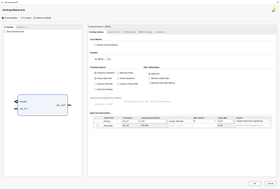
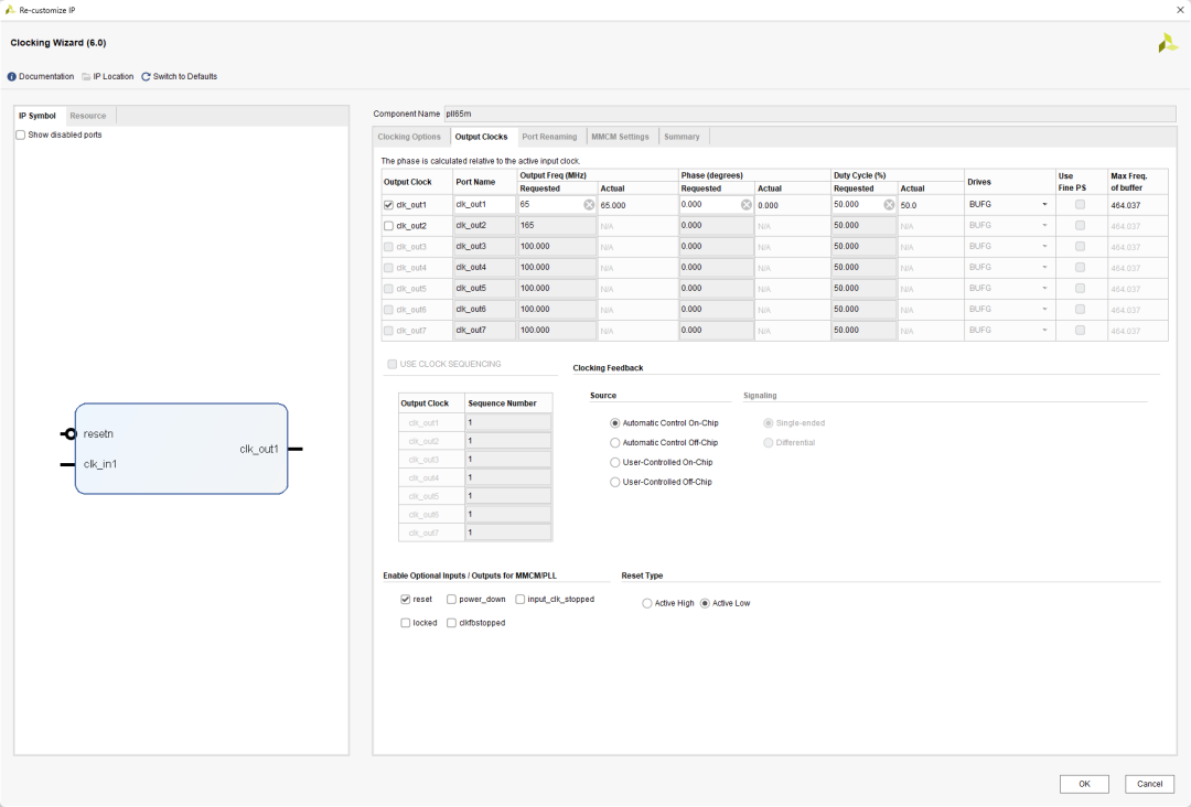
The clock is the core of the FPGA system. To avoid metastability and ensure reliable data transmission, the design gives priority to ensuring that the clocks of all modules are homologous; for asynchronous clock domains, FIFO is used for buffering. In view of the frequency difference between the DAC904 and AD9226 devices, this design adopts a frequency reduction strategy, adjusting the operating frequency of the DAC904 to 65 MHz, consistent with the AD9226, thereby achieving global clock synchronization. Since the development board only provides a 125 MHz onboard clock, a frequency divider must be used to extract the required 65 MHz operating clock from it.
The specific configuration parameters of the Clocking Wizard IP core in this design are as follows:
The AM/ASK demodulation in this design adopts the envelope demodulation method, specifically as follows:

The source code of the AM/ASK demodulation module is:
module AM_Demodulation(
input wire clk_65m,
input wire rst_n,
input wire signed [11:0] data,
output wire [13:0] AM_ASK_data
// ================= Envelope extraction part =================
wire signed [11:0] abs12 = data[11] ? (~data + 1'b1) : data;
wire signed [15:0] abs16 = {abs12, 4'b0000};
wire signed [15:0] lpf_out16;
AM_LPF envelope_filter (
.clk_enable(1'b1),
.filter_in(abs16),
.filter_out(lpf_out16)
// assign env_out_16 = lpf_out16;
//================= Output waveform logic =================
reg signed [13:0] AM_ASK_data_reg;
wire signed [13:0] env_for_dac = lpf_out16[15:2];
always @(posedge clk_65m or negedge rst_n) begin
if (!rst_n) begin
AM_ASK_data_reg <= 14'sd0;
AM_ASK_data_reg <= env_for_dac;
wire signed [13:0] AM_gain = 14'd20;
wire signed [13:0] AM_ASK_data_reg_out = AM_ASK_data_reg << 4;
assign AM_ASK_data = {~AM_ASK_data_reg_out[13], AM_ASK_data_reg_out[12:0]}-14'd3300;
//.clk(clk_65m), // input wire clk
//.probe0(data), // input wire [11:0] probe0
//.probe1(env_out_16) // input wire [15:0] probe1
The rectification process is actually very simple: take the average value and then pad the high bits to match the input bit width of the filter.
Among them, AM_LPF uses a 1st-order low-pass IIR Butterworth filter with a sampling frequency of 65000 kHz and a cutoff frequency of 100 kHz. The specific parameters are generated by the fdatool in MATLAB, and the specific configuration is shown below:
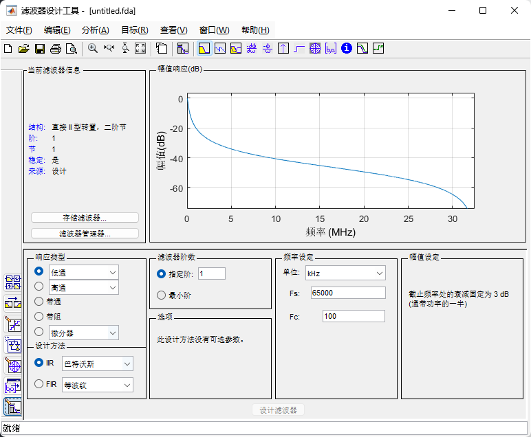
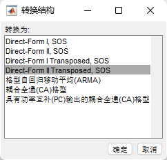
Note: Set it to Direct-Form II Transposed, second-order sections. Click Design Filter. After obtaining the filter, click Edit -> Convert Structure -> Direct-Form II Transposed, SOS at the top until the filter structure conversion is complete. Click the quantization parameters setting in the lower-left corner, set the filter arithmetic to fixed-point, and finally click Apply. After quantization is complete, click Targets -> Generate HDL... at the top to open the filter generation tool. Select Verilog as the language, set Reset asserted level in Global Settings to Active-low (because all resets in this system are active-low), then choose the location for filter generation and locate the corresponding .v file.
V. VIVADO ROM IP Core
ROM is the abbreviation of Read-Only Memory. It is a solid-state semiconductor memory that can only read data stored in advance. Its characteristic is that once data is stored, it cannot be changed or deleted, and the data will not be lost when the power is turned off. In fact, the ROM or RAM generated by IP cores in FPGA calls the internal RAM resources of the FPGA, and the contents are lost when power is removed. The ROM module generated by the IP core only adds a data file (.coe format) in advance, and initializes the ROM module through the data file when the FPGA is running. https://blog.csdn.net/yishuihanq/article/details/130767125
In the sine wave generation architecture based on DAC904, the discrete nature of the digital domain determines the staircase effect of the analog output. Since DAC904 has a 14-bit resolution, its digital input code can represent =16384 quantization levels. Combined with its ±5V reference range (10V peak-to-peak), the minimum quantization step size (LSB) of the system is calculated as follows:
This means that for every incremental digital code output by the FPGA, the analog voltage changes by only about 0.6mV. A standard full-scale sine wave, with its peak corresponding to +5V (digital code 16383) and its trough corresponding to -5V (digital code 0 or two's complement form), will contain 16384 discrete level sampling points over the entire cycle.
For waveform data generation, I used software developed by someone whose identity I no longer remember; if there is any infringement, please contact me. You can also directly generate the coe file with MATLAB. Note whether the dataset is signed or unsigned. Link: https://pan.baidu.com/s/1XYoQW VR FX-wA8fMdy-slvA?pwd=1111 Extraction code: 1111
We generally use MATLAB to pre-generate the required waveform data (usually a full-scale waveform, i.e., equal to the depth), store it in a coe file, configure the ROM core accordingly, and then the waveform data can be stored in the program and called afterward.
This module adopts a digital phase-locked frequency discrimination loop structure, mainly including a numerically controlled oscillator, a phase detector, a low-pass filter, and a loop filter.
Numerically controlled oscillator module: composed of a ROM IP core and a phase accumulator. Through the input frequency control word and phase control word, it controls the ROM IP core to output cosine reference signals of different frequencies and phases.
Phase detector module: implemented with a multiplier. The input signal is multiplied by the local cosine signal to produce the phase detector output, which includes a low-frequency error and a double-frequency component. In the program, the high bits of the multiplication result are first taken, and then sent to the filter to remove the high-frequency part, leaving only the phase error.
Low-pass filter module: still a 1st-order low-pass IIR Butterworth filter, with a sampling frequency of 65MHz and a cutoff frequency of 100kHz.
Loop filter module: after low-pass filtering, the phase error enters the loop filter module to generate a frequency control quantity. This frequency control quantity is used both for NCO frequency offset adjustment and as the FM/FSK demodulation result output. The specific parameters (C1, C2) need to be adjusted according to actual conditions.
module FM_demodulation(
input signed [11:0] data,
output [13:0] FM_FSK_data
// At a 65MHz sampling rate, 1MHz = (1e6/65e6) * 2^32 ≈ 66076419
localparam [31:0] PHASE_STEP_1MHZ = 32'd66076419; // Center frequency 1MHz
localparam [31:0] INITIAL_FREQ = PHASE_STEP_1MHZ; // Initial frequency 1MHz
wire [11:0] phase_addra;
wire signed [11:0] cos_out;
wire signed [23:0] pd_mult_out; // Phase detector (multiplier) output
wire signed [31:0] freq_control; // Loop filter output (frequency control word)
wire signed [15:0] lpf_out_full; // Low-pass filter output
wire signed [11:0] phase_error; // Phase error after truncation
// ================= Loop filter module =================
// Receives the phase detection error and outputs the frequency control word to control the NCO
loop_filter_FM loop_filter_inst (
.theta(phase_error), // Input phase error
.delta(freq_control) // Output frequency adjustment quantity (this signal is the FM demodulation result)
// ================= NCO (Numerically Controlled Oscillator) =================
PhaseAccumulator nco (
.PhaseOffset(12'd0),
.PhaseStep(INITIAL_FREQ + $unsigned(freq_control)), // Track the input signal frequency
.MemAddr(phase_addra)
// Generate local carrier (FM PLL only needs one cosine or sine channel for phase detection)
rom_sin_12bit cos_rom (
.addra(phase_addra + 12'd1024), // cos phase offset
.douta(cos_out)
// Convert the unsigned offset binary code output from ROM to signed two's complement