Imaging Processing with FPGA
Embed the widget on your own site
Add the following snippet to your HTML:
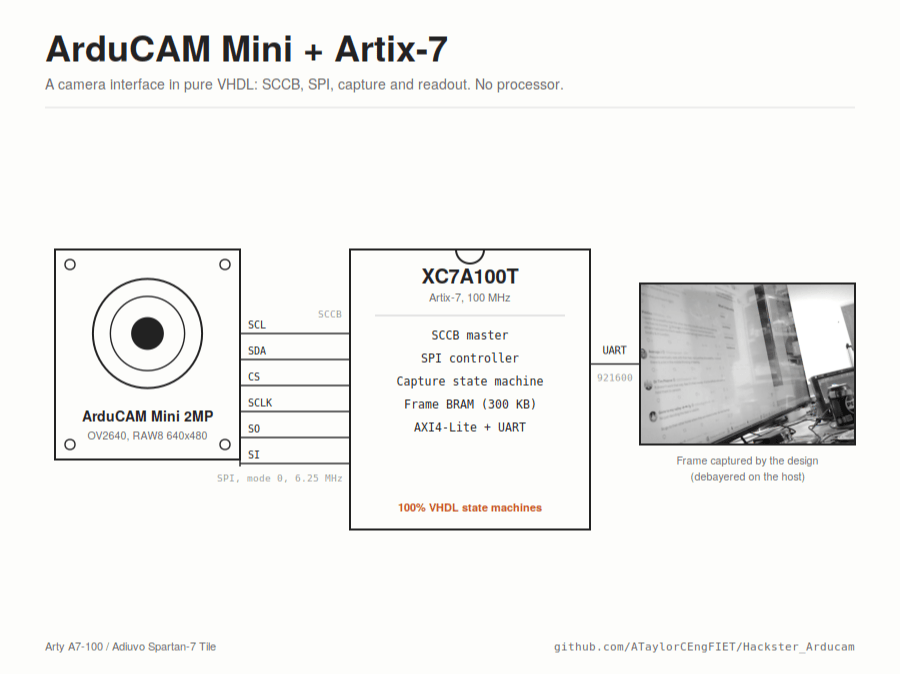
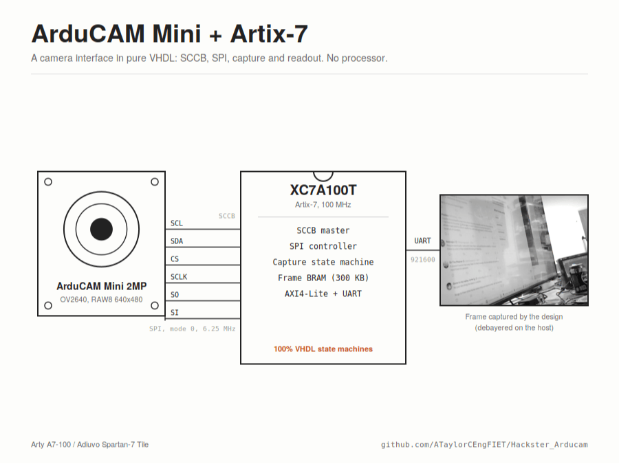
Interfacing the ArduCAM Mini OV2640 with an FPGA using nothing but VHDL state machines: SCCB configuration, SPI capture, BRAM frame storage
Read up about this project on
ArduCAM Mini Meets the FPGA: A Pure-Logic VHDL Solution

Things used in this project
Hardware components
Software apps and online services
Image processing is one of the areas where FPGAs really shine, but getting pixels into the device in the first place is often the hardest part of any project. MIPI cameras need specialised PHY handling; parallel DVP sensors consume a lot of pins and require careful timing closure, and both usually end up with a processor somewhere in the loop running configuration software.
The ArduCAM Mini takes a different approach, which makes it very attractive for FPGA development. The module pairs an OmniVision OV2640 sensor with an ArduChip, which buffers a complete frame in an on-module FIFO and presents the whole camera behind just two simple interfaces: SCCB (essentially I2C) for sensor configuration and SPI for control and pixel readout. That means we can capture images using a handful of Pmod pins and some straightforward digital logic.
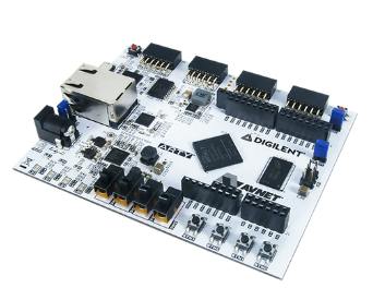
In this project, we are going to develop a complete camera interface in VHDL with no processor and no soft core anywhere in the design. The FPGA configures the sensor, runs the capture sequence, self-tests the links, stores the frame and serves it to a host. The project targets the Digilent Arty A7-100 as the validated platform, with an additional streaming variant for the Adiuvo Spartan-7 Tile which sends live frames to a Raspberry Pi over SPI.
All of the source, scripts, testbenches and validated bitstreams are available on GitHub, so you can program a board and capture a frame without even opening Vivado.
The ArduCAM Mini
The ArduCAM Mini 2MP provides the OV2640 sensor, which outputs frames over its parallel DVP interface to the ArduChip. The ArduChip handles all of the pixel-clock-domain timing internally and writes the frame into its FIFO. From our side of the connector, life is much simpler. We talk to two devices:
The OV2640 sensor is configured over SCCB. This is where we set the output format, resolution, exposure and gain behavior. For this project, the sensor is configured for RAW8 Bayer output at 640 by 480, which gives us one byte per pixel and a frame of exactly 307, 200 bytes.
The ArduChip is controlled over SPI. Its register set lets us reset the capture logic, flush the FIFO, trigger a single-frame capture, poll for completion, read the captured length and finally burst-read the pixel data out of the FIFO.
This split is what makes the module such a good fit for pure-logic implementation. There is no continuous pixel stream to keep up with; the frame sits patiently in the ArduChip FIFO until we are ready to drain it at whatever rate our SPI clock supports.
Design Overview
The repository retains three synthesizable designs, all built on the same underlying camera controller:
An AXI4-Stream output version, which presents captured pixels as an 8-bit AXI4-Stream with TUSER marking start of frame and TLAST marking end of line. This is the natural choice if you want to drop the camera into an existing video pipeline.
A single-frame BRAM capture version for the Arty A7-100, which stores the frame in block RAM and makes it available over AXI4-Lite, accessed from a host PC through a 921, 600 baud UART bridge. This is the validated hardware target and the focus of this project.
A streaming version for the Adiuvo Spartan-7 Tile (XC7S25), which drops the full-frame buffer entirely and streams pixels to a Raspberry Pi over an 8 MHz SPI link. We will look at this towards the end.
The Arty design is assembled in IP Integrator. The arducam_bram_if block contains the SCCB master, the ArduChip SPI controller, the capture state machine and an AXI4-Lite slave. A UART protocol bridge converts simple command packets from the host into AXI reads and writes, which means the PC can inspect status registers and read the frame buffer word by word with no processor in the loop. An AXI GPIO provides the capture enable. The frame buffer appears at address 0x0000_0000, with control at 0x4000_0000 and the status, FIFO length and ArduChip version registers at 0x4001_0000 onwards.
SCCB and SPI in Logic
Two small controllers sit at the bottom of the design.
The SCCB master implements the OmniVision variant of I2C as a single state machine. It supports 8- and 16-bit register addresses (the OV2640 uses 8-bit banked registers, while the OV5642 uses 16-bit addresses, and the design supports both sensors through a generic), drives SCL and SDA open drain through IOBUF primitives at the top level, and reports done and error status back to the sequencer. The bus runs at a comfortable rate set by a clock divisor generic, 250 by default from the 100 MHz system clock.
The SPI controller is a mode 0 master with a programmable divisor. With the default divisor the SPI clock is 6.25 MHz — well within the ArduChip's capabilities, and forgiving of flying leads on a Pmod. The controller supports the hold-CS behavior needed for the ArduChip burst read, where the command byte is followed by an arbitrary number of data bytes in a single chip-select assertion.
The Capture Sequence
The heart of the design is the capture-state machine, which runs the entire bring-up and capture sequence that would normally live in Arduino library code.
The sequence is deliberately paranoid, with self tests built in at every stage. After a start-up wait, the ArduChip is reset and released through register 0x07. We then write 0x55 to the ArduChip test register and read it back; if the scratch test fails, the SPI wiring or mode is wrong and there is no point continuing, so the error flag is raised and the sequence stops. The ArduChip version register is read and reported through AXI for good measure.
Next the sensor itself is verified over SCCB. For the OV2640, we select register bank one and read the chip ID from registers 0x0A and 0x0B, expecting 0x2642. Only once both links have proven themselves does the state machine walk the OV2640 configuration table, setting up RAW8 VGA output with automatic exposure and gain control enabled, a 16x AGC ceiling and 50 Hz banding filter.
One practical lesson from hardware testing is worth highlighting: automatic exposure needs time to converge. The first capture after configuration was consistently dark until a settle period was added. The design waits one second (a generic, g_aec_settle_clks, defaulting to 100, 000, 000 clocks at 100 MHz) after sensor setup before the first capture, which gives the AEC loop time to react to the scene. If your application needs a faster start, this is the knob to turn.
The capture itself follows the standard ArduChip recipe: flush the FIFO and clear the flags, trigger a single-frame capture, poll the trigger register until the done bit sets, then read the three FIFO length registers and sanity check the result against the expected 307, 200 bytes. Finally, a single burst read streams every pixel into the frame buffer BRAM, the frame-ready status bit is set and the LEDs on the Arty report init done and frame ready.
Talking to the Board
With the frame sitting in BRAM, the host side is refreshingly simple. The UART bridge accepts small command packets for single-word reads and writes, so the entire host application is a Python script using PySerial.
The script polls the status register until init done and frame ready are both set (the status word also carries the sensor ID and SPI scratch readback, so a failed self test is immediately visible from the PC), verifies the FIFO length, then reads the frame 64 words at a time:
python scripts\read_frame_uart.py COM6 --output frame_capture The script writes out the raw Bayer data, a grayscale BMP and a bilinearly debayered color BMP. At 921, 600 baud a full VGA frame takes a few seconds to transfer, which is perfectly acceptable for a single-frame capture design.
Connecting the Hardware
The camera connects to Pmod JA on the Arty A7-100. The module is 3.3 V only, so do not be tempted by anything higher.
The UART runs over the Arty's existing USB-UART bridge, so no additional wiring is needed on the host side. The SCCB lines are driven open drain through IOBUF primitives instantiated explicitly in the top level, relying on the module pull-ups.
Before any hardware was touched, the design was verified against behavioral models of both sensors. The repository includes self-checking test-benches which model the OV2640 and OV5642, including the SCCB register banks, the ArduChip register behavior and the FIFO burst read. Both simulations run from a single script:
powershell -ExecutionPolicy Bypass -File scripts\run_xsim.ps1 The test-benches check the full sequence end to end: they verify the configuration writes arrive correctly, respond to the ID reads with the expected values, and supply a known pixel pattern which the test-bench then checks at the output. A Questa flow is also provided for those who prefer it.
On hardware, an ILA was included in the validated build, and the checked-in.ltx probe file plus a set of Tcl scripts allow the SPI transactions to be captured and decoded from the running design, which proved invaluable when bringing up the SPI mode and burst timing.
Streaming to a Raspberry Pi
The BRAM design captures one frame at a time, which is ideal for stills but not for live video. The third variant in the repository targets the Adiuvo Spartan-7 Tile, a small XC7S25 board, and takes a different approach: it removes the full-frame buffer completely.
Instead of 300 KB of frame storage, the design keeps only a 4 KiB pixel FIFO in block RAM. Pixels are packed into 32-bit words and served to a Raspberry Pi as 256-byte bursts using an AXI protocol engine behind an SPI slave. A data-ready line on GPIO24 tells the Pi when a chunk is available, and crucially the back-pressure works all the way through: if the Pi pauses, the ArduCAM FIFO drain pauses too, so nothing overflows and no full-frame RAM is ever needed. After exactly 307, 200 bytes have been consumed, the next frame starts automatically.
The Pi side is again a simple Python application using spidev. Each 256-byte pixel read is a single 274-byte full-duplex SPI transaction: a burst-read command, a big-endian address, a beat count, some dummy bytes to cover the protocol response latency, and then the pixel data. With the camera-side SPI at 6.25 MHz, the camera read is the throughput limit, giving a theoretical maximum of around 2.5 frames per second for VGA RAW8 before software overhead. Not video rates, but a genuinely live image from a 25 K logic cell part with room to spare: the implemented design uses around 40 percent of the LUTs and a single block RAM tile.
powershell -ExecutionPolicy Bypass -File scripts\build_adiuvo_s7_25_spi_project.ps1 python3 scripts/read_frame_spi_pi.py
This project shows that a complete camera system, from sensor configuration through capture to host delivery, fits comfortably in pure logic. The ArduCAM Mini's architecture does us a big favor by hiding the pixel-clock domain behind its FIFO, leaving two simple, slow interfaces which map naturally onto compact VHDL state machines. Along the way we picked up a few transferable lessons: build self tests into bring-up sequences so faults are diagnosed by the design itself, give automatic exposure time to settle before trusting the first frame, and let back-pressure do the work of a frame buffer when streaming.
From here the AXI4-Stream variant is the obvious starting point for real image processing pipelines, with the captured Bayer data feeding demosaicing, filtering or detection logic in the fabric.
The complete project, including sources, test-benches, build scripts and validated bitstreams for both boards, is available at https://github.com/ATaylorCEngFIET/Hackster_Arducam

Related channels and tags