FPGA PCIe Pin Assignment Guide
When you get a Xilinx FPGA board, the first thing to focus on is how to perform PCIe pin assignment in Vivado.
There are many shortcuts: some reliable development board vendors (such as Digilent) provide comprehensive constraint files (.xdc). We only need to add it to the Vivado project and then comment out the pin assignments we don't use. For example, the NetFPGA constraint file can be downloaded here:
https://digilent.com/reference/_media/reference/programmable-logic/netfpga-sume/sume_master.zip.
But in many cases (especially for non-official boards), these are not provided, so we need to use a general method — read the development board PCB schematic and write the .xdc ourselves for pin assignment.
Taking NetFPGA as an example, download its schematic at https://digilent.com/reference/_media/reference/programmable-logic/netfpga-sume/netfpga-sume_sch.pdf.
On the schematic, you can find all the components on the board. First, we need to find the PCIe connector component (i.e., the PCIe gold fingers, used to plug into the PCIe slot on the computer motherboard). Figure 1 shows what the PCIe connector looks like in the schematic. We should focus on the following:
PCIe differential signal lines in both TX (transmit) and RX (receive) directions
A pair of differential clock lines (REFCLK)
A reset line (PERST#)
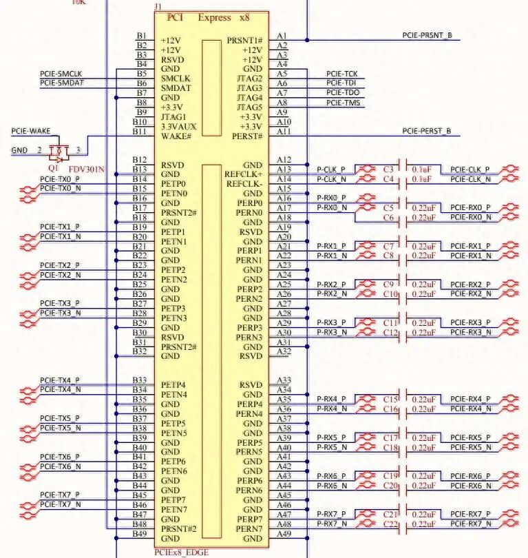
Figure 1: The PCIe connector component (commonly known as gold fingers) in the NetFPGA schematic. (From page 1 of the NetFPGA schematic)
From Figure 1, we can see that this is a PCIe x8 connector, because there are 8 pairs of differential signal lines in each direction. On the left side of Figure 1, we see:
TX direction differential pair 0, with net names PCIE-TX0_P and PCIE-TX0_N in the figure;
TX direction differential pair 1, with net names PCIE-TX1_P and PCIE-TX1_N in the figure;
And so on... there are 8 pairs of TX differential lines in total.
RX direction differential pair 0, with net names PCIE-RX0_P and PCIE-RX0_N in the figure;
RX direction differential pair 1, with net names PCIE-RX1_P and PCIE-RX1_N in the figure;
And so on... there are 8 pairs of RX differential lines in total.
PCIe specifies a pair of differential reference clock signals (REFCLK), which are provided by the RC (e.g., computer motherboard) to the EP (FPGA) to drive the PCIe core inside the EP. In Figure 1, the net names are PCIE-CLK_P and PCIE-CLK_N.
PCIe specifies a reset signal (PERST#), which is provided by the RC to the EP to reset the system. In Figure 1, the net name is PCIE-PESET_B.
Note!!! A very important thing is to figure out which side the TX (transmit) and RX (receive) signal directions are referenced to. The RC's (host's) TX is RX for the EP (FPGA); the RC's RX is TX for the EP. The person drawing the schematic may name the signal lines according to their own preference — some call the RC's TX "TX", while others call the EP's TX "TX", which can easily confuse readers.
A reliable way to distinguish them is to look at the pin arrangement on the PCIe connector component: the PCIe reference clock (REFCLK) and reset (PERST#) are always on the same side as the RC's RX (EP's TX).
For example, in Figure 1, the reference clock and reset are on the right side, so the differential signal lines on the right side are all RC's RX, meaning the direction is from the FPGA to the computer motherboard. The differential signals on the left side are all RC's TX, meaning the direction is from the computer motherboard to the FPGA.
Obviously, the person who drew this schematic has a habit of naming TX and RX from the RC's perspective. However, in FPGA development, we are accustomed to the opposite—naming TX and RX from the FPGA's perspective. This point should be noted when writing the constraint file (.xdc) later.
The perspective issue of RX and TX often causes many developers to "capsize in a ditch." For FPGA developers, it's simply a matter of correcting the constraints in the .xdc file. But for PCB design, once a mistake is made, that board revision is ruined.
After confirming the above information, the next step is to locate the FPGA pins corresponding to these signals in the schematic and obtain the package pin numbers of these pins, so as to write the constraint file (.xdc).
These signals may be connected directly from the PCIe connector to the FPGA pins, but they may also pass through some components (such as resistors, capacitors, level-shifting chips, etc.) along the way. These intermediate components are irrelevant to us; we just need to trace all the way to the corresponding FPGA pin.
For example, if we search the schematic for a net named PCIE-TX0_P, we can immediately find the locations where all PCIe differential signal pairs and clock pairs connect to the FPGA, as shown in Figure 2.
First, we need to confirm that what we have found is indeed the FPGA (and not an intermediate component along the signal path). The way to do this is to check the label on it. In Figure 2, the label at the bottom reads XC7VX690T-3FFG1761I, which is indeed the FPGA model corresponding to the NetFPGA development board—no problem.
Then we need to note the FPGA pin numbers corresponding to these lines. For example, in Figure 2, PCIE-TX7_P corresponds to pin number AG6, PCIE-TX7_N corresponds to pin number AG5, and so on…
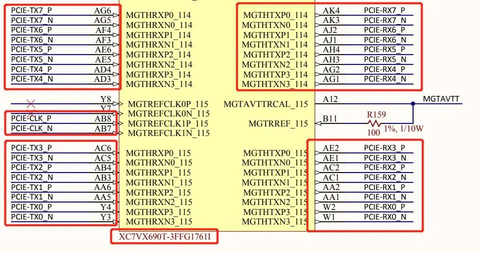
Figure 2: Locations in the NetFPGA schematic where PCIe signal lines and clock lines connect to the FPGA. (Excerpted from page 12 of the NetFPGA schematic)
Figure 2 covers all PCIe x8 signals and one pair of clocks, but does not include the PCIe reset signal (PERST). If we search the schematic for the net name PCIE-PESET_B corresponding to the reset signal, we will first find a component SN74AVC4T245, as shown in Figure 3 (a quick online search reveals that this is a level-shifting chip).
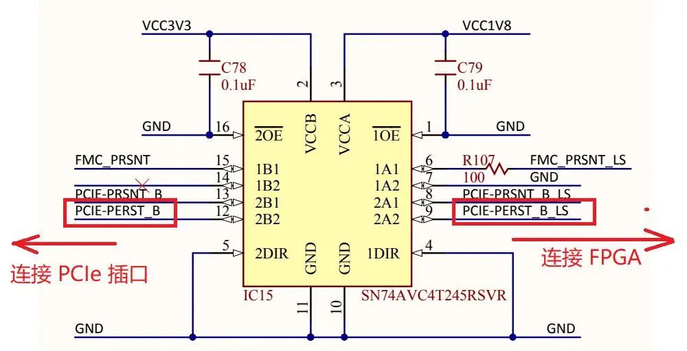
Figure 3: The level-shifting component on the PCIe reset signal path. (Excerpted from page 7 of the NetFPGA schematic)
Then, by continuing to search using the net name PCIE-PERST_B_LS, we can find the location where the reset signal connects to the FPGA chip, as shown in Figure 4. We can see that the FPGA pin number corresponding to the PCIe reset signal is AY35.
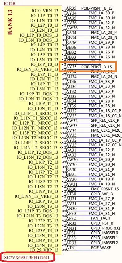
Figure 4: Location in the NetFPGA schematic where the PCIe reset line connects to the FPGA. (Excerpted from page 7 of the NetFPGA schematic)
Based on the pin numbers we found in Figure 2 and Figure 4, the PCIe pin constraint file (.xdc) for NetFPGA should be as follows:
# NetFPGA PCIe-related pin constraints ----------------------------------------------------------------------------------------
set_property -dict { PACKAGE_PIN AY35 IOSTANDARD LVCMOS18 PULLUP true } [get_ports i_pcie_rstn]; # PCIe reset
set_property PACKAGE_PIN AB8 [get_ports { i_pcie_refclkp }]; # PCIe differential clock
set_property PACKAGE_PIN W2 [get_ports { o_pcie_txp[0] }]; # PCIe differential signal (FPGA side TX pair 0)
set_property PACKAGE_PIN AA2 [get_ports { o_pcie_txp[1] }]; # PCIe differential signal (FPGA side TX pair 1)
set_property PACKAGE_PIN AC2 [get_ports { o_pcie_txp[2] }]; # PCIe differential signal (FPGA side TX pair 2)
set_property PACKAGE_PIN AE2 [get_ports { o_pcie_txp[3] }]; # PCIe differential signal (FPGA side TX pair 3)
set_property PACKAGE_PIN AG2 [get_ports { o_pcie_txp[4] }]; # PCIe differential signal (FPGA side TX pair 4)
set_property PACKAGE_PIN AH4 [get_ports { o_pcie_txp[5] }]; # PCIe differential signal (FPGA side TX pair 5)
set_property PACKAGE_PIN AJ2 [get_ports { o_pcie_txp[6] }]; # PCIe differential signal (FPGA side TX pair 6)
set_property PACKAGE_PIN AK4 [get_ports { o_pcie_txp[7] }]; # PCIe differential signal (FPGA side TX pair 7)
set_property PACKAGE_PIN Y4 [get_ports { i_pcie_rxp[0] }]; # PCIe differential signal (FPGA side RX pair 0)
set_property PACKAGE_PIN AA6 [get_ports { i_pcie_rxp[1] }]; # PCIe differential signal (FPGA side RX pair 1)
set_property PACKAGE_PIN AB4 [get_ports { i_pcie_rxp[2] }]; # PCIe differential signal (FPGA side RX pair 2)
set_property PACKAGE_PIN AC6 [get_ports { i_pcie_rxp[3] }]; # PCIe differential signal (FPGA side RX pair 3)
set_property PACKAGE_PIN AD4 [get_ports { i_pcie_rxp[4] }]; # PCIe differential signal (FPGA side RX pair 4)
set_property PACKAGE_PIN AE6 [get_ports { i_pcie_rxp[5] }]; # PCIe differential signal (FPGA side RX pair 5)
set_property PACKAGE_PIN AF4 [get_ports { i_pcie_rxp[6] }]; # PCIe differential signal (FPGA side RX pair 6)
set_property PACKAGE_PIN AG6 [get_ports { i_pcie_rxp[7] }]; # PCIe differential signal (FPGA side RX pair 7)
PACKAGE_PIN is followed by the pin number corresponding to this pin.
Xilinx specifies that for differential pairs (including differential clocks and differential signals), only the P side needs to be constrained and the N side does not need to be constrained. Therefore, i_pcie_refclkn, o_pcie_txn, and i_pcie_rxn do not appear in the .xdc file.
The TX and RX in the schematic (Figure 2) are from the perspective of the RC. In the .xdc, we recommend using the FPGA's perspective, which is opposite to the RC's perspective. Therefore, o_pcie_txp[0] in the .xdc corresponds to PCIE-RX0_P in the schematic, and so on...
NetFPGA provides a PCIe x8 width. In practice, we can use narrower x1 and x4 widths, in which case we need to comment out the unused pins in the .xdc.
For example, when using only PCIe x1, you should comment out o_pcie_txp[1~7] and i_pcie_rxp[1~7]; only keep o_pcie_txp[0] and i_pcie_rxp[0].
The IOSTANDARD LVCMOS18 for the PCIe reset signal means the pin's voltage level is 1.8V CMOS. The PCIe clock and signal pins do not require an IOSTANDARD specification.
PULLUP true for the PCIe reset signal means the pin is weakly pulled up to a high level. Not specifying PULLUP true here should not affect functionality, but I haven't tried it yet.
For the above .xdc constraint file, the module definition in the top-level Verilog file of the FPGA project should be as follows. Note:
The pin names in the .xdc should be kept consistent with those in the Verilog.
For a differential signal pair, both P and N signals appear in the Verilog. Unlike in the .xdc, where only P needs to be constrained.
// Definition of the Verilog top-level module for the FPGA project module fpga_top ( // PCIe-related signals input wire i_pcie_rstn, input wire i_pcie_refclkp, i_pcie_refclkn, input wire [7:0] i_pcie_rxp, i_pcie_rxn, output wire [7:0] o_pcie_txp, o_pcie_txn, // Other function-related signals // ....);
Every pin on every chip has a pin number. Most FPGAs today use BGA packages, as shown in Figure 5. The underside has a pin array, starting from one corner of the chip, with each column named by letters (A, B, C, D, ..., X, Y, Z, AA, AB, ...) and each row named by a number (1, 2, 3, ..., 8, 9, 10, ...). Therefore, pin AB8 refers to the pin in column AB, row 8.
Original title: FPGA PCIe Pin Assignment
A Brief Discussion on How to Overcome FPGA I/O Pin Assignment Challenges
On the Issue of FPGA Pin Assignment
FPGA Tcl Pin Assignment Issues
How to Use a Multi-Point Signal to Assign a PCIe Clock?
How to Use a Multi-Point Signal to Assign a PCIe Clock?
A Beginner with an FPGA Development Board: How to Get Started with Pin Assignment
How to Overcome FPGA I/O Pin Assignment Challenges?
FPGA Pin Signal Assignment Principles Every Engineer Must Know
How to Assign FPGA Pin Signals? Several Basic Principles of FPGA Pin Assignment
MagicSOPC Motherboard FPGA-IO Pin Assignment Table
XILINX FPGA Hardware Design Summary: PCIe Hardware Design Pitfall Avoidance Guide
How to Optimize Clock Assignment in PCIe Applications
A Brief Discussion on Several Principles of FPGA Pin Signal Assignment