Bringing Enterprise Development Flow into Classroom: Xiaoyanjing Tech FPGA Industry-Education Course at Guangzhou City Institute of Technology
Recently, a four-day "Integrated Circuit Industry-Education Integration Practice" FPGA hands-on course concluded successfully at the School of Electronic Information Engineering and Communication, Guangzhou City Institute of Technology. Jointly organized by Xiaoyanjing Tech and Guangzhou City Institute of Technology, the training closely aligns with the development trends of the domestic FPGA industry, using Pango Microsystems' Logos2 series chips as the core platform. It innovatively integrates the full enterprise-level development flow, engineering standards, and acceptance criteria into teaching, achieving a seamless connection from classroom theory to industry practice. The training aims to deepen the alignment between university talent cultivation and industry needs, effectively enhancing students' engineering practice capabilities and system design thinking, and delivering professionals with hands-on engineering expertise to the integrated circuit field. 01
Course Content: The training course is designed according to the approach of "digital fundamentals first, tools upfront, interface hands-on practice, system integration," with content progressing from basic to advanced levels, fully covering the complete domestic FPGA development chain, and is divided into five major teaching modules. 01 FPGA Hardware Architecture and Digital Circuit Fundamentals. The course systematically explains the internal resource composition of Pango Microsystems' Logos2 series FPGAs, including programmable logic units, programmable IOBs, routing resources, and hard-core resources such as BRAM, PLL, and DSP. Using a "4-to-1 multiplexer" as a teaching case, the course analyzes the lookup-table principle of LUT-based combinational logic implementation, clarifying the intrinsic mechanism by which "FPGA structures contain no gate circuits yet can implement gate circuits." On this basis, the course compares hardware design flow with FPGA design flow item by item, mapping out the complete correspondence from schematic, netlist, and PCB layout and routing to RTL, synthesis, place-and-route, and bitstream generation, helping students build hardware design thinking of "what circuit the code corresponds to." 02 Verilog Syntax and Coding Standards. The course systematically covers fundamental syntax including identifiers, four logic values (0/1/x/z), wire and register types, operators and precedence, with emphasis on distinguishing combinational logic from sequential logic. The course provides in-depth explanation of the hardware implications of non-blocking assignments, the consequences of misusing blocking assignments, and the correspondence between reg types and registers. The course also establishes coding standards such as port naming prefixes, active-low designations, clock naming, and Latch avoidance, helping students avoid common engineering issues such as unintended latch inference, cross-clock-domain sampling anomalies, and timing corruption, and building hardware parallel design thinking. 03 PDS Toolchain and Simulation Debugging. The course comprehensively outlines the standardized PDS development flow: creating a project, adding source code, compilation and synthesis, device mapping, place-and-route, bitstream generation, and download configuration, with extended coverage of Flash programming, including bitstream conversion, external Flash scanning, and power-off auto-start mechanisms. The simulation section systematically explains ModelSim environment setup, Testbench writing methods, and .do script automation flows, clarifying the necessity of scripted simulation in engineering practice; the debugging section details the collaborative mechanism of Inserter and Debugger tools, enabling automatic insertion of debug cores into the netlist and JTAG online trigger acquisition, effectively solving the real-board debugging challenge of "simulation passes but the board behaves abnormally." 04 Interface Hands-on Practice: HDMI, I2C, and DDR3. Using the HDMI display path as the guiding thread, the course works through three key interfaces item by item.
The course provides a detailed explanation of the TMDS (Transition Minimized Differential Signaling) mechanism, analyzes the configuration flow of the MS7200 receiver chip and MS7210 transmitter chip, uses ColorBar as the minimum verifiable path, and implements each item in conjunction with VESA DMT standard timing parameters. The I2C bus section explains the physical definition of START/STOP, the modeling differences between Moore and Mealy state machines, and the timing parameter calculation method for deriving the target rate from the system clock, and clarifies the timing necessity of "dummy write address, repeated START" in read operations. The DDR3 section analyzes the configuration and Example Design of the HMIC_S IP, demonstrates the capacity basis for using DDR3 rather than on-chip BRAM for 720p frame buffering, and explains the burst transfer mechanism. 05 Signal Processing and System Integration systematically explains the sampling theorem and aliasing phenomenon, the three-step ADC conversion of sampling—quantization—encoding, the DAC restoration mechanism, as well as the FPGA implementation paths of the DDS signal source (phase accumulator, sine lookup table, DAC) and FFT transformation. The course-concluding system integration project integrates all knowledge points to complete the development of an integrated hardware system, including five major functions: HDMI image acquisition, DDR3 image frame buffering, DDS sine wave generation, ADC signal sampling, and FFT spectrum analysis. During the hands-on process, emphasis is placed on overcoming engineering challenges such as PLL clock configuration, cross-clock-domain CDC synchronization, I2C chip initialization, FIFO data stream buffering, and online waveform debugging, ultimately realizing a complete physical system that displays superimposed images and waveform spectra. 02

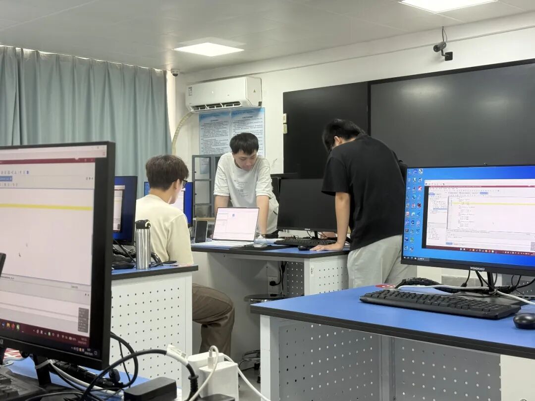
On-site and Feedback This course adopted a teaching mode that advanced "theoretical instruction, in-class hands-on practice, and one-on-one Q&A" simultaneously, with students independently completing project setup, simulation verification, and board-level testing according to the lecture notes. The classroom discussion atmosphere was strong. At the end of the course, we collected learning feedback from some of the students. Students generally stated that this course broadened their technical horizons, and that they not only mastered practical development skills but also established rigorous engineering design thinking.
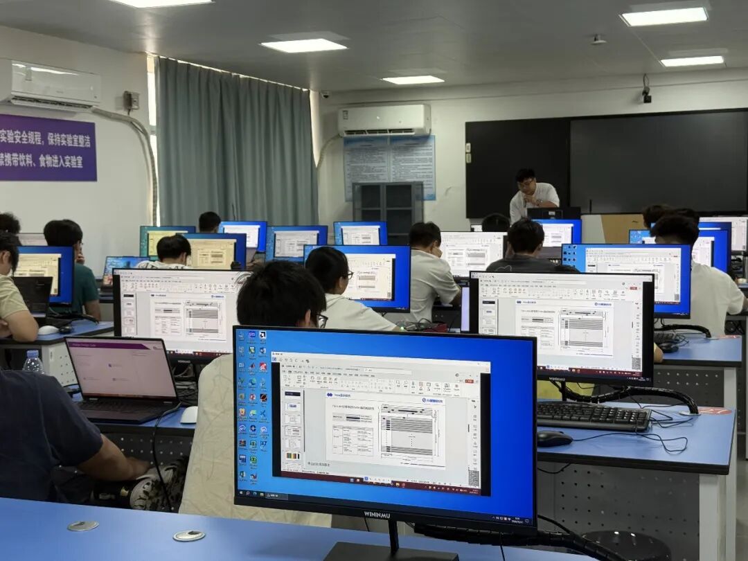
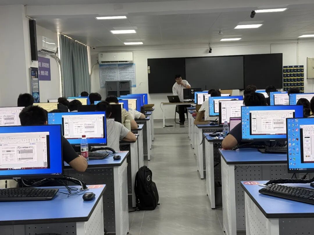
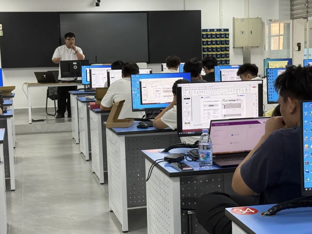
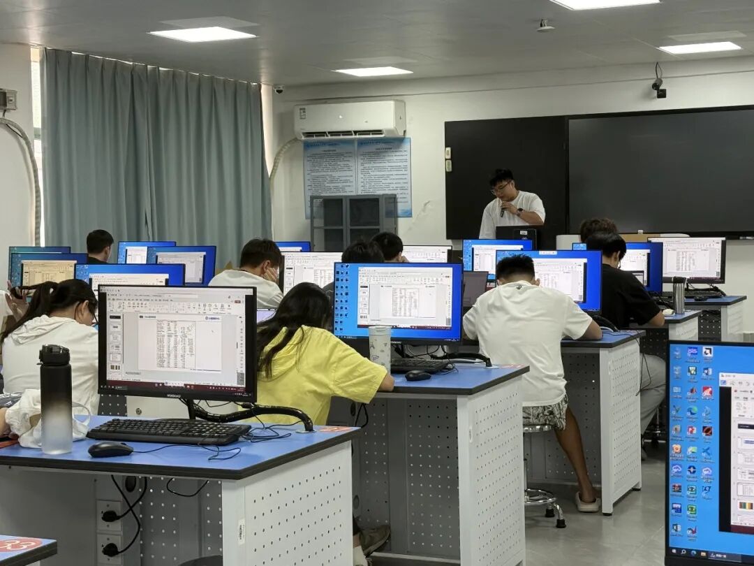
"The teacher's lectures were very humorous. I used to feel that FPGA was especially far away from me, but after listening to the teacher's class I realized it was not that scary. He broke down complex principles and explained them thoroughly, and always used examples from daily life as analogies. After explaining, he would take us to verify on the board, one link after another, so it was impossible to lose focus."
"What I gained the most from was the online debugging part. Previously, when doing course projects, if the simulation passed but the board did not work, I could only stare blankly at the board. This time I learned to use the Debugger to set trigger conditions and capture I2C waveforms. For the first time I saw with my own eyes START, address, ACK, and data bits lined up in sequence on the waveform. That feeling of finally understanding was so exhilarating!"
"The biggest change over the 4 days is that I dare to open manuals now. Previously, when encountering an unfamiliar chip, I would first search for tutorials. Now I first go to datasheets and standard documents—VESA timing tables, I2C specifications. The answers are actually all in there; I just did not know where to look before..."
"I must praise the teacher's patience. Sometimes our questions were really quite 'beginner-level,' but the teacher answered seriously every time and would conveniently connect the related knowledge points as well. During the afternoon lab sessions, the teacher kept walking around the classroom, going to whoever was stuck and teaching hand by hand until they got it."
"What impressed me most was the DDR3 lesson. I previously did not understand why the entire frame image could not be put into BRAM. The teacher calculated the capacity and then explained burst transfer and bit width, and it suddenly became clear. It turns out that choosing a storage solution has to be calculated, not decided by gut feeling."
Deepening University-Enterprise Cooperation and Jointly Building a New Ecosystem of Industry-Education Integration As an active promoter of the industry-education integration ecosystem for domestic FPGAs and AI, Xiaoyanjing Tech relies on the dual-engine drive of "industry empowerment + education integration." Through the "Xiaoyanjing Tech University Program," it has joined hands with leading chip companies such as Pango Microsystems to build a domestic FPGA practical platform close to real industrial scenarios, and has actively integrated into the Ascend AI ecosystem, launching an end-to-end acceleration solution for "AI+FPGA" heterogeneous collaboration. It transforms more than ten years of deep industry experience in engineering implementation into a standardized teaching system, and uses a full-chain collaborative model of "teaching—competition—research—industry" to bridge the "last mile" between talent cultivation and industry demand. In the future, the company will continue to deepen industry-education integration with major universities, bring more domestic FPGA practical projects close to the industrial frontier, Ascend AI deployment courses, and systematic teaching systems into campuses, jointly build a bridge between theory and practice with university teachers and students, and continuously supply high-quality innovative engineering talent to the domestic integrated circuit and AI ecosystem.
Fanyi Education and Hunan Institute of Technology Explore New Paths for Cultivating Electronic Information Talent
Hubei Polytechnic University Procures DZ-TGA101 Thermogravimetric Analyzer from Nanjing Dazhan
Focus on FPGA Hands-on Practice! Xiaoyanjing Tech Empowers 2026 Jiangsu Vocational College IC Application Development Competition Teacher Training Program!
Computing Power Reconstruction, Boundless Intelligent Innovation | Xiaoyanjing Tech Shines with Hardcore Solutions at 2026 Pango Developer Conference!
Passing the Torch of Chip Innovation, Walking Together in Industry-Education | Xiaoyanjing Tech Appointed Council Member of the National IC Industry-Education Integration Community!
Xiaoyanjing Tech Delivers FPGA Summer Course at Beijing University of Posts and Telecommunications
Passing the Torch of Chip Innovation, Walking Together in Industry-Education | Xiaoyanjing Tech Invited to IC Science-Education-Industry Integration Symposium
Gathering at GEB, Embarking on a New Journey | Xiaoyanjing Tech Showcases Multiple Core Product Solutions at the 64th China Higher Education Expo
DWIN University-Enterprise Cooperation Project Recognized as 2025 Typical Case of Electronic Information Industry-Education Integration
Chip Competition, Cloud Power! Xiaoyanjing Tech Launches Remote AI Experiment Platform to Boost 2026 IC Innovation Competition!
New Benchmark for Industry-Education Integration: Xiaoyanjing Tech Helps Inaugurate BIT-Pango Domestic FPGA Course-Competition Integration Laboratory!
From Lecture Notes to Academy: Qian Xuesen's 1963 "Interstellar Blueprint" and Its Echoes in 2026
Industry-Education Integration, Collaborative Innovation: 2025 DWIN University Program Achievements Review
2025 Ascend AI Technology Seminar · Hangzhou Station Grandly Opens! Xiaoyanjing Tech Invites You to Witness AI+FPGA Empowering the New Ascend Ecosystem!
Dongguan University of Technology "Xiaoyanjing Tech Cup" 4th IC Design and Innovative Application Competition Successfully Concludes