800MB/s! Swiss Company Shows How to Implement High-Speed FPGA Data Acquisition
In the field of high-speed test and measurement, data acquisition capabilities continue to improve, and the pressure on system design increases accordingly.
Multiple data streams input continuously, the FPGA needs to perform real-time processing and data scheduling, the processor is responsible for system control, and storage devices must keep up with data write speeds. A bottleneck in any one of these links can affect the operating efficiency of the entire device.
For equipment developers, the truly difficult challenges are often not just performance issues. How to complete hardware design, low-level software adaptation, and system integration within a limited development cycle while controlling development risks is the key to whether a project can be successfully implemented.
Enclustra's AMD Zynq UltraScale+ data logger project provides a highly representative solution approach.
The project uses the Enclustra Mercury+ XU8 SoM to build a high-speed data acquisition and storage platform, ultimately achieving continuous measurement data recording and access capability of 800 MB/s. More notably, the Mercury+ XU8 not only handles core processing tasks but also shortens the development path for the entire system through an integrated hardware architecture, abundant high-speed interfaces, and mature software support.
This is also where the value of an FPGA SoM lies: it does not merely provide chip computing power, but helps customers more quickly build an embedded system that can truly be put into application.
I. Starting from a core board to lower the development threshold for high-speed measurement equipment
In traditional FPGA system development, engineers not only need to complete logic design but also must handle the complex relationships among processors, DDR memory, power supplies, clocks, high-speed interfaces, and peripheral devices.
For designs based on MPSoC, these tasks especially test the team's hardware experience. Low-level circuit design, signal integrity verification, and hardware-software integration all require time investment. Once a design problem occurs, re-verification or even hardware modification may affect project progress.
The value of the Mercury+ XU8 lies first in integrating these key resources onto a compact SoM.
The Mercury+ XU8 is based on the AMD Zynq UltraScale+ MPSoC and integrates programmable logic, an ARM processor system, high-speed DDR4 memory, eMMC, QSPI Flash, as well as resources such as dual Gigabit Ethernet and dual USB 3.0. The module also provides high-speed interface capabilities such as PCIe Gen3 and PCIe Gen2, and brings out abundant user I/O through onboard connectors. Specific resources depend on the selected device model.
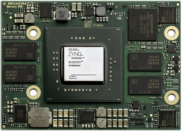
Combined, these resources mean that customers do not need to build a complete MPSoC hardware platform from scratch but can instead develop carrier boards and dedicated functions around the actual application.
For a high-speed data logger, the carrier board is mainly responsible for connecting the core module with the SSD, external acquisition interfaces, and other peripheral devices; FPGA logic and processor software then work together on this basis.
The significance of this modular design is not just reducing a few components, but moving part of the complex low-level hardware development and verification work forward onto a mature platform.
For R&D teams, doing less repetitive low-level work means more time can be spent on acquisition links, data processing, and product functions.
Especially for companies that need to quickly complete prototype verification, develop dedicated measurement equipment, or upgrade existing systems, this approach can reduce initial development investment and also help reduce the risks brought by redesign.
II. FPGA and ARM collaboration allows high-speed data processing and system management to each perform their own roles
A high-speed data logger is not simply a storage device. After data enters the system, it requires not only high-speed, parallel data processing capability but also an operating system to provide functions such as file management, device control, and network communication. Having a single processing unit handle all tasks is not necessarily the most suitable architecture.
The Mercury+ XU8 is based on the Zynq UltraScale+ MPSoC, integrating programmable logic (PL) and a processing system (PS) in the same module, providing a foundation for hardware-software co-design.
In this data logger, FPGA logic is used to build data processing and buffering paths suitable for application requirements, while the integrated processor system runs Linux and is responsible for software tasks such as SSD data reading and writing.
This division of labor has practical significance. The FPGA can customize hardware logic based on data stream characteristics and process different data channels in parallel; the processor can leverage a mature operating system and software ecosystem to handle file systems, network control, and device management. Engineers do not need to rely on software for every task, nor must they hardwire all functions into hardware logic.
The independent PS and PL memory channels provided by the Mercury+ XU8 also offer flexibility in memory configuration for different processing tasks. Depending on the specific model, the module can support up to 8 GB of PS-side DDR4 ECC SDRAM and up to 4 GB of PL-side DDR4 SDRAM.
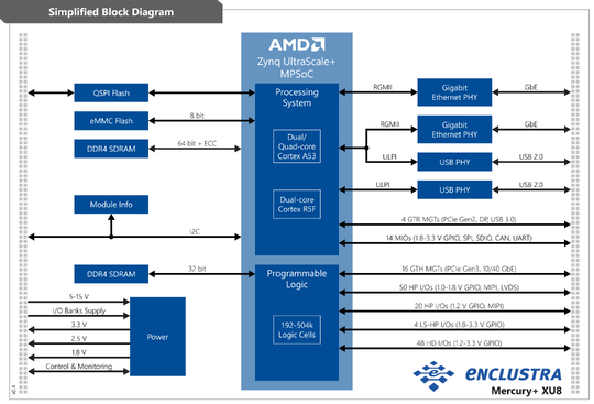
It should be noted that memory bandwidth, FPGA logic resources, and actual data throughput are different metrics and cannot be simply equated. Final performance still depends on the data path design, interface configuration, caching strategy, and the overall performance of the storage system.
But from an architectural perspective, the Mercury+ XU8 provides an important foundation for such systems: enabling hardware parallel processing and software system management to work together on the same platform.
3. The key to 800 MB/s lies not only in the SSD, but also in the complete data path
This data logger ultimately achieved 800 MB/s of sustained measurement data recording and access capability, using two hot-swappable SATA SSDs.
For FPGA engineers, what is noteworthy about this result is not just the speed itself, but how the system handles continuously incoming data.
One of the worst-case scenarios for high-speed acquisition systems is when the front end continuously generates data while the back-end storage speed fluctuates. If the data stream does not have sufficient buffer space, even a short-term rate mismatch can cause buffer overflow and compromise acquisition integrity.
Therefore, data buffering is a critical part of the overall system design.
In this project, Enclustra used its own Stream Buffer Controller IP core to temporarily store measurement data awaiting writes to the SSD through a virtual FIFO mechanism. This IP core can simultaneously manage up to 16 independent data streams and supports up to 4 GB of storage capacity.
This allows the system to provide more flexible buffering and data stream management before data enters the storage device.
For customers, the value of a mature IP core is not just saving RTL development time. It also reduces the work of repeatedly implementing common functions, allowing engineers to focus on system interface adaptation, cache parameter configuration, data integrity verification, and actual application performance optimization.
Of course, caching cannot compensate for long-term bandwidth shortages. The system still needs to be designed holistically based on the data generation rate, sustained SSD write capability, and cache capacity.
The Mercury+ XU8 provides the hardware foundation for programmable logic and processors to work together, while the mature IP core further helps the development team turn this foundation into a concrete high-speed data logging system.
The combination of these two is one of the key technical paths that enabled this project to achieve high throughput.
4. Mature software support means customers do not have to start from the ground up
Hardware performance determines what a system can achieve, while the software ecosystem affects how much effort engineers need to put in to make it happen.
The Mercury+ XU8 provides a Linux BSP and the corresponding development toolchain. The project team used these foundational software supports to let the Linux system handle SSD data read/write tasks and adopted the Ext4 file system to store log data.
This may appear to be routine software configuration, but it is very important for real projects.
If a team needs to handle low-level boot processes, memory adaptation, and peripheral device drivers on its own, the development cycle can easily be stretched by these non-core tasks. Using a mature BSP can reduce repetitive low-level adaptation work and allow software development to move faster into the application phase.
At the same time, the project adopts a software architecture based on C# and ASP.NET Core, implements remote network control through a Web API, and uses a local Web GUI based on ASP.NET MVC and Razor Pages to assist system debugging.
In this way, the data logger is no longer just a hardware device capable of receiving data, but a complete device that can integrate into the customer's existing network and measurement systems.
For applications such as industrial testing, automated measurement, and laboratory data acquisition, this system integration capability is equally important. Whether a device can be controlled by a host computer and whether it can work with existing software often directly affects the actual user experience of the product.
The advantage of Mercury+ XU8 lies precisely in the fact that it provides both hardware resources and a corresponding software development foundation, helping teams move faster from the underlying platform to application implementation.
V. Interfaces and architecture leave margin for future product upgrades
The performance requirements of measurement equipment will not remain at the current level forever.
As sampling rates, channel counts, and data resolution continue to increase, systems may require larger caches, higher interface bandwidth, or faster storage devices. If the original architecture lacks room for expansion, subsequent upgrades may involve hardware modifications on a larger scale.
The high-speed interface resources of Mercury+ XU8 provide flexibility for further design of such systems. Depending on the specific model and interface configuration, the module supports resources such as PCIe Gen3, PCIe Gen2, USB 3.0, Gigabit Ethernet, and multiple high-speed transceivers, which can be used to build different types of high-speed data transmission and peripheral connection solutions.
In this project, the system uses a SATA SSD for data recording while retaining the possibility of future upgrades to NVMe SSDs.
This does not mean that performance will necessarily increase proportionally after replacing the storage device. Actual upgrades still require evaluation of the interface implementation, data movement path, software stack, and storage device performance. However, considering storage technology evolution in advance can reduce the pressure of re-planning the entire system architecture in the future.
For equipment developers, this design approach helps extend the service life of the product platform. At the current stage, product development can be completed around clear requirements, and targeted upgrades can be made in the future according to customer application and data throughput requirements.
For module suppliers, being able to provide customers with a SoM that has multiple interface resources, mature software support, and a scalable design foundation also means that it is not just a one-time hardware purchase, but may become a common platform for subsequent product series.
VI. The value of Mercury+ XU8 is to help customers move faster toward product deployment
From this case, the value of Mercury+ XU8 cannot be measured solely by FPGA logic resources or the peak bandwidth of a single interface.
It integrates the AMD Zynq UltraScale+ MPSoC, processing system, programmable logic, high-speed storage resources, and rich interfaces onto a compact module, and combined with the Linux BSP and Enclustra IP cores, helps the project team establish the hardware and software foundation required for a high-speed data recording system.
This solution ultimately achieved 800 MB/s continuous measurement data recording and access capability, and also demonstrated the practical role of a modular FPGA platform in the development of complex embedded devices.
For FPGA engineers, Mercury+ XU8 provides a flexible platform that can be used to build high-speed data processing systems; for equipment manufacturers, it can reduce part of the underlying hardware and software development work, allowing teams to focus more on the core functions of their own products.
What is truly worth noting is not only how high a data throughput Mercury+ XU8 can support, but how it helps customers integrate FPGA performance, processor software capabilities, and peripheral storage systems to shorten the distance from hardware design to equipment delivery.
In the fields of high-speed test and measurement, data acquisition, and industrial embedded systems, the value of this kind of platform that balances performance, development efficiency, and subsequent scalability is becoming increasingly important.
Hardware timestamp support, a new domain controller high-speed PCIe data acquisition and recording solution #IntelligentDrivingTesting #PCIeBusDebugging #DomainController #DataAcquisition
Implementing S7, Modbus TCP, and OPC UA data acquisition based on Node-RED
An upgrade practice for an electric energy data acquisition terminal
A new-generation electric energy data acquisition terminal solution
A data acquisition practice based on FPGA and LabVIEW
Measured 300 MB/s! DSMC bus enables RK3572+ FPGA high-speed interconnection
Ruiqing Platform | DSMC+ FPGA communication speed increased to 90 MB/s

Portable high-speed synchronous AD data acquisition card
Deeply engaged in high-speed data acquisition, GaGe: Vitrek's high-performance hardcore brand
Leveraging AI assistance -> Designing an FPGA-based data acquisition system
Independently developing a high-speed data acquisition system
FPGA-based DAQ system | Challenges in achieving high-performance data acquisition
How Pico oscilloscopes achieve multi-channel synchronous acquisition
PCIe data acquisition card design schematic: 138 - 1-channel 1Gsps AD, 1-channel 1Gsps DA high-speed acquisition, storage and playback device
High-speed slitting machine PLC data acquisition remote monitoring system solution